


LCD CONTROLLER/DRIVER S3C9228/P9228
13-6
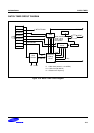
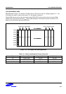
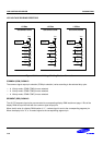
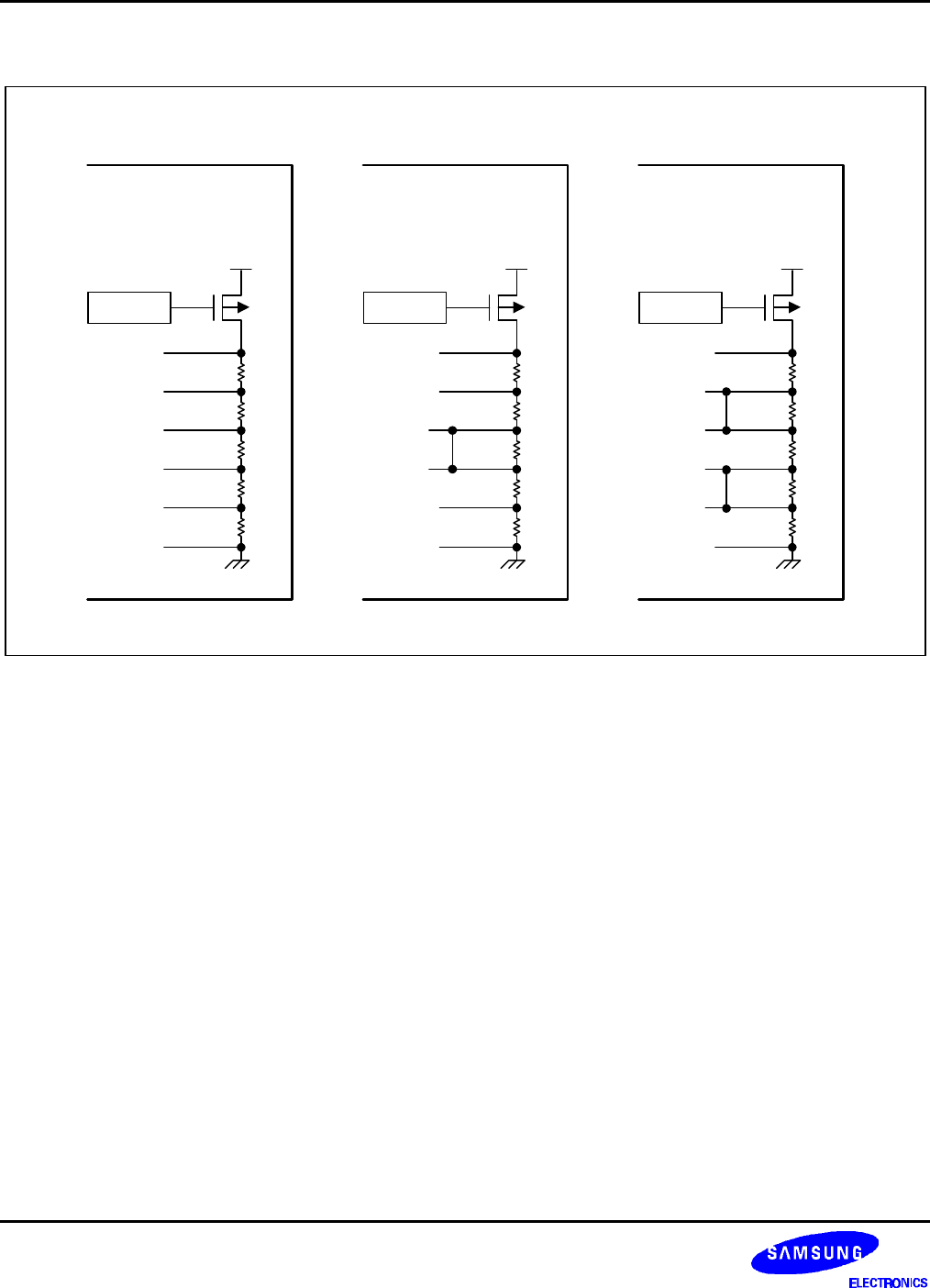
LCD VOLTAGE DIVIDING RESISTORS
1/5 Bias
S3C9228/P9228
VDD
R
R
R
R
R
LMOD.4
VLC1
VLC2
VLC3
VLC4
VLC5
VSS
1/4 Bias
S3C9228/P9228
VDD
R
R
R
R
R
LMOD.4
VLC1
VLC2
VLC3
VLC4
VLC5
VSS
1/3 Bias
S3C9228/P9228
VDD
R
R
R
R
R
LMOD.4
VLC1
VLC2
VLC3
VLC4
VLC5
VSS
Figure 13-6. Internal Voltage Dividing Resistor Connection
COMMON (COM) SIGNALS
The common signal output pin selection (COM pin selection) varies according to the selected duty cycle.
— In 1/3 duty mode, COM0-COM2 pins are selected
— In 1/4 duty mode, COM0-COM3 pins are selected
— In 1/8 duty mode, COM0-COM7 pins are selected
SEGMENT (SEG) SIGNALS
The 19 LCD segment signal pins are connected to corresponding display RAM locations at page 1. Bits of the
display RAM are synchronized with the common signal output pins.
When the bit value of a display RAM location is "1", a select signal is sent to the corresponding segment pin.
When the display bit is "0", a 'no-select' signal to the corresponding segment pin.