


System Introduction 1-41
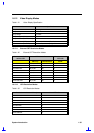
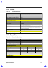
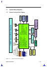
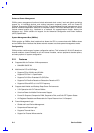
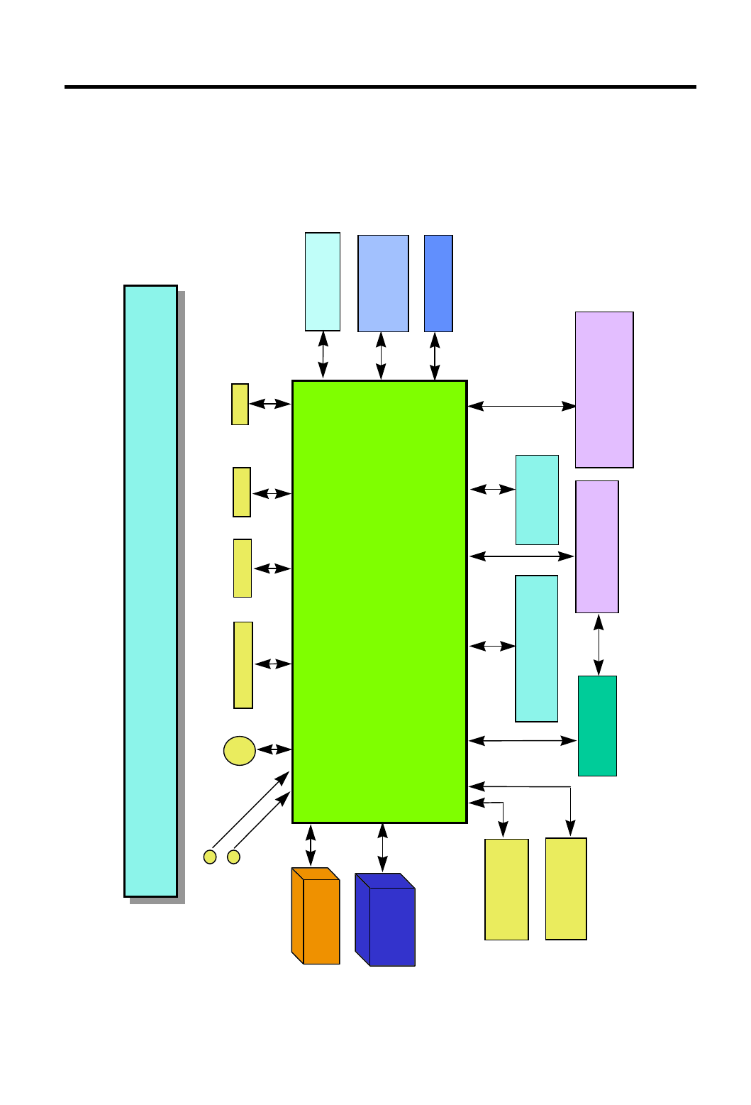
1.7 System Block Diagrams
1.7.1 System Functional Block Diagram
“7100” System Block Diagram
MAIN BOARD
.
Intel Tillamook/Deschutes MMO
.
PCI IDE
.
Intel 430TX Core Logic chipset
.
NS87338 Super I/O controller
.
512KB L2 cache memory
.
256KB PMU/System/Video BIOS
.
32~128MB EDO/SDRAM memory
.
6832 CardBus chip
.
NeoMagic NMG4 VGA chip
.
IBM IrDA/FIR
.
2MB video memory
.
DMI 2.0 with Intel LDCM
Ext. Keyboard
or PS/2 Mouse
6-pin
25-pin
15-pin
9-pin
Parallel
Port
CRT
Port
Serial
Port
DC-DC
Converter
DC-AC
Inverter
12.1” SVGA TFT,
13.3” XGA TFT
2.5” 12.7mm HDD
3.0GB+
45w
AC Adapter
Pri-Battery
84/85-key
auto-tilt-up
Keyboard
10.8V 5500mAh Li-Ion
3P3S (10w/cell) 3.6V/cell
100V ~ 240V
Auto-Switching
Touchpad
Charger
68-pin
Two CardBus
Slots
240-pin
Docking
Line-in jack
Line-out jack
soDIMM x 2
32~128MB
Swappable FDD,
CD-ROM, removable
3” HDD module
Figure 1-13 System Functional Block Diagram