


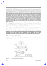

2-14 Service Guide
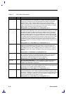
Table 2-2 82371AB Pin Descriptions
Name Type Description
KBCCS#/
GPO26
O
KEYBOARD CONTROLLER CHIP SELECT. KBCCS# is asserted during I/O
read or write accesses to KBC locations 60h and 64h. It is driven combinatorially
from the ISA addresses SA[19:0] and LA[23:17]. If the keyboard controller does
not require a separate chip select, this signal can be programmed to a general
purpose output.
During Reset: High After Reset: High During POS: High/GPO
MCCS# O
MICROCONTROLLER CHIP SELECT. MCCS# is asserted during I/O read or
write accesses to IO locations 62h and 66h. It is driven combinatorially from the
ISA addresses SA[19:0] and LA[23:17].
During Reset: High After Reset: High During POS: High
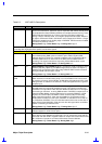
PCS0#
PCS1#
O
PROGRAMMABLE CHIP SELECTS. These active low chip selects are asserted
for ISA I/O cycles which are generated by PCI masters and which hit the
programmable I/O ranges defined in the Power Management section. The X-Bus
buffer signals (XOE# and XDIR#) are enabled while the chip select is active. (i.e.,
it is assumed that the peripheral which is selected via this pin resides on the X-
Bus.)
During Reset: High After Reset: High During POS: High
RCIN# I
RESET CPU. This signal from the keyboard controller is used to generate an
INIT signal to the CPU.
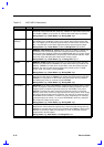
RTCALE/
GPO25
O
REAL TIME CLOCK ADDRESS LATCH ENABLE. RTCALE is used to latch the
appropriate memory address into the RTC. A write to port 70h with the
appropriate RTC memory address that will be written to or read from causes
RTCALE to be asserted. RTCALE is asserted on falling IOW# and remains
asserted for two SYSCLKs. If the internal Real Time Clock is used, this signal
can be programmed as a general purpose output.
During Reset: Low After Reset: Low During POS: Low/GPO
RTCCS#/
GPO24
O
REAL TIME CLOCK CHIP SELECT. RTCCS# is asserted during read or write
I/O accesses to RTC location 71h. RTCCS# can be tied to a pair of external OR
gates to generate the real time clock read and write command signals. If the
internal Real Time Clock is used, this signal can be programmed as a general
purpose output.
During Reset: High After Reset: High During POS: High/GPO
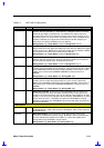
XDIR#/
GPO22
O
X-BUS TRANSCEIVER DIRECTION. XDIR# is tied directly to the direction
control of a 74’245 that buffers the X-Bus data, XD[7:0]. XDIR# is asserted
(driven low) for all I/O read cycles regardless if the accesses is to a PIIX4
supported device. XDIR# is asserted for memory cycles only if BIOS or APIC
space has been decoded. For PCI master initiated read cycles, XDIR# is
asserted from the falling edge of either IOR# or MEMR# (from MEMR# only if
BIOS or APIC space has been decoded), depending on the cycle type. For ISA
master-initiated read cycles, XDIR# is asserted from the falling edge of either
IOR# or MEMR# (from MEMR# only if BIOS space has been decoded),
depending on the cycle type. When the rising edge of IOR# or MEMR# occurs,
PIIX4 negates XDIR#. For DMA read cycles from the X-Bus, XDIR# is driven low
from DACKx# falling and negated from DACKx# rising. At all other times, XDIR#
is negated high. If the X-Bus not used, then this signal can be programmed to be
a general purpose output.
During Reset: High After Reset: High During POS: High/GPO