


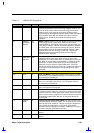
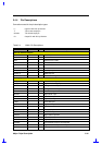
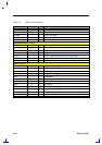
Major Chips Description 2-37
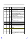
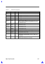
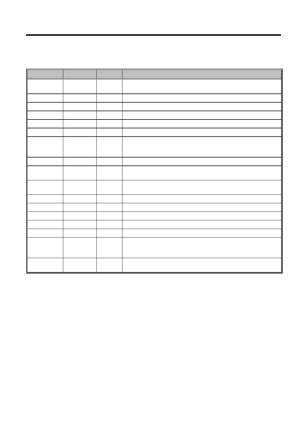
Table 2-3 NM2160 Pin Descriptions
Number Pin name I/O Description
136, 154,
173
DVSS DRAM ground
105 AVSSM Analog ground for MCLK synthesizer
104 AVSSV Analog ground for VCLK synthesizer
99 AVSSR1 Analog ground for DAC
100 AVSSR2 Analog ground for DAC current reference
91 AVSSX1 Analog ground for crystal oscillator
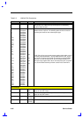
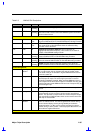
25, 42, 57,
78
HVDD
Host bus interface VDD.(+5v or +3v) Includes the PCI, VL, CRT,
Power management, External clock pins(PMCLKI and PVCLKI)
and Miscellaneous pins
27,62,107 VDD Logic VDD(+3V only)
134, 156,
175
DVDD DRAM VDD(+3V only)
116, 132, 1,
8
LVDD Panel VDD(+5v or +3v)
157 MMVDD ZV Port VDD(+5V /+3V)
106 AVDDM Analog VDD for MCLK synthesizer(+3V only)
103 AVDDV Analog VDD for VCLK synthesizer(+3V only)
95 AVDDR1 Analog VDD for DAC(+3V only)
102 AVDDR2 Analog VDD for DAC current reference(+3V only)
94 AVDDX1
Analog VDD for crystal oscillator. If external 14 MHz source is
used AVDDX1 can be +5V or +3V based on the XTAL1 clock
source levels
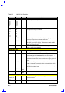
133 VBB A capacitor across ground to this pin is required. Please refer to
NM2160 system schematics for more details