


Major Chips Description 2-21
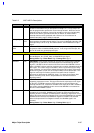
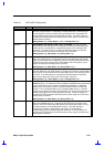
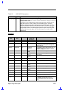
Table 2-2 82371AB Pin Descriptions
Name Type Description
SDA[2:0] O
SECONDARY DISK ADDRESS[2:0]. These signals indicate which byte in either
the ATA command block or control block is being addressed. If the IDE signals
are configured for Primary and Secondary, these signals are connected to the
corresponding signals on the Secondary IDE connector. If the IDE signals are
configured for Primary Master and Primary Slave, these signals are used for the
Primary Slave connector.
During Reset: High-Z After Reset: Undefined During POS: SDA
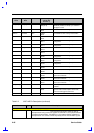
SDCS1# O
SECONDARY CHIP SELECT FOR 170H-177H RANGE. For ATA command
register block. If the IDE signals are configured for Primary and Secondary, this
output signal is connected to the corresponding signal on the Secondary IDE
connector. If the IDE signals are configured for Primary Master and Primary
Slave, these signals are used for the Primary Slave connector.
During Reset: High After Reset: High During POS: High
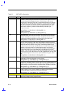
SDCS3# O
SECONDARY CHIP SELECT FOR 370H-377H RANGE. For ATA control register
block. If the IDE signals are configured for Primary and Secondary, this output
signal is connected to the corresponding signal on the Secondary IDE connector.
If the IDE signals are configured for Primary Master and Primary Slave, these
signals are used for the Primary Slave connector.
During Reset: High After Reset: High During POS: High-Z
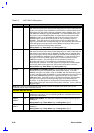
SDD[15:0] I/O
SECONDARY DISK DATA[15:0]. These signals are used to transfer data to or
from the IDE device. If the IDE signals are configured for Primary and Secondary,
these signals are connected to the corresponding signals on the Secondary IDE
connector. If the IDE signals are configured for Primary Master and Primary
Slave, these signals are used for the Primary Slave connector.
During Reset: High-Z After Reset: Undefined During POS: SDD
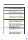
SDDACK# O
SECONDARY DMA ACKNOWLEDGE. This signal directly drives the IDE device
DMACK# signal. It is asserted by PIIX4 to indicate to IDE DMA slave devices that
a given data transfer cycle (assertion of SDIOR# or SDIOW#) is a DMA data
transfer cycle. This signal is used in conjunction with the PCI bus master IDE
function. It is not associated with any AT compatible DMA channel. If the IDE
signals are configured for Primary and Secondary, this signal is connected to the
corresponding signal on the Secondary IDE connector. If the IDE signals are
configured for Primary Master and Primary Slave, these signals are used for the
Primary Slave connector.
During Reset: High After Reset: High During POS: High
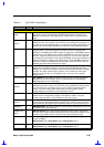
SDDREQ I
SECONDARY DISK DMA REQUEST. This input signal is directly driven from the
IDE device DMARQ signal. It is asserted by the IDE device to request a data
transfer, and used in conjunction with the PCI bus master IDE function. It is not
associated with any AT compatible DMA channel. If the IDE signals are
configured for Primary and Secondary, this signal is connected to the
corresponding signal on the Secondary IDE connector. If the IDE signals are
configured for Primary Master and Primary Slave, these signals are used for the
Primary Slave connector.