


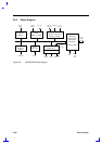
2-58 Service Guide
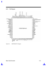
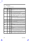
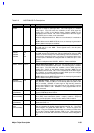
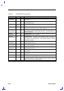
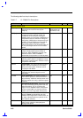
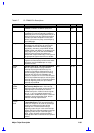
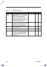
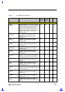
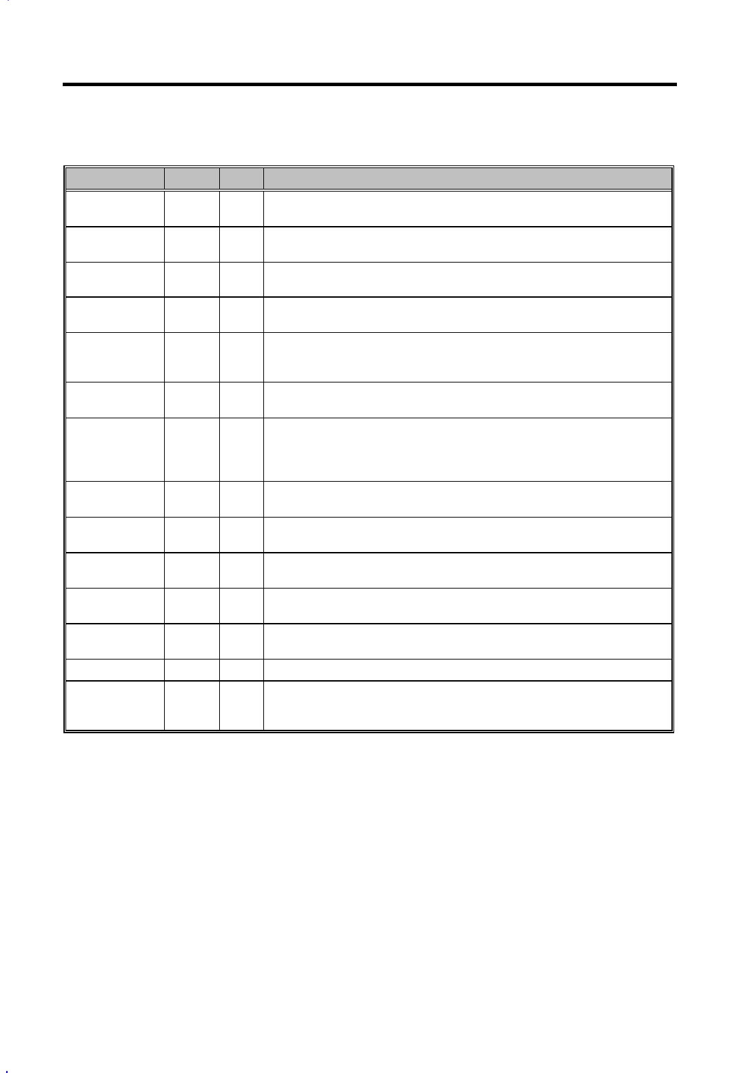
Table 2-6 NS97338VJG Pin Descriptions
Pin No. I/O Description
/TRK0
(PPM Mode)
91 I
FDC Track 0. This pin gives an additional Track 0 signal in PPM Mode
when PNF = 0.
VDDB, C 48, 97
Power Supply. This is the 3.3V/5V supply voltage for the
PC87332VJG circuitry.
VSSB-E 40, 7,
88, 59
Ground. This is the ground for the PC87332VJG circuitry.
/WAIT 82 I
EPP Wait. This signal is used in EPP mode by the parallel port device
to extend its access cycle. It is an active low signal.
/WDATA
(Normal Mode)
37 O
FDC Write Data. This output is the write precompensated serial data
that is written to the selected floppy disk drive. Precompensation is
software selectable.
/WDATA
(PPM Mode)
81 O
FDC Write Data. This pin provides an additional Write Data signal in
PPM Mode when PNF=0. (See PE.)
/WGATE
(Normal Mode)
36 O
FDC Write Gate. This output signal enables the write circuitry of the
selected disk drive. WGATE has been designated to prevent glitches
during power-up and power-down. This prevents writing to the disk
when power is cycled.
/WGATE
(PPM Mode)
80 O
FDC Write Gate. This pin gives an additional Write Gate signal in
PPM mode when PNF = 0.
/WP
(Normal Mode)
34 I
FDC Write Protect. This input indicates that the disk in the selected
drive is write protected.
/WP
(PPM Mode)
90 I
FDC Write Protect. This pin gives an additional Write Gate signal in
PPM mode when PNF = 0.
/WR 16 I
Write. An active low input to signal a write from the microprocessor to
the controller.
/WRITE 93 O
EPP Write Strobe. This signal is used in EPP mode as write strobe. It
is active low.
X1 5 I
Clock. Active clock input signal of 14.318 MHz, 24MHz or 48MHz.
/ZWS 1 O
Zero Wait State. This pin is the Zero Wait State open drain output pin
when bit 6 of FCR is 0. ZWS is driven low when the EPP or ECP is
written, and the access can be shortened.