


Major Chips Description 2-69
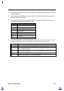
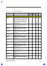
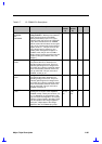
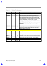
Table 2-7 CL-PD6832 Pin Descriptions
Pin Name Description Pin No.
(socket
A)
Pin No.
(socket
B)
I/O Power
BVD1/
-STSCHG/
-RI/
-CSTSCHG
Battery Voltage Detect 1 / Status Change
/ Ring Indicate: In Memory Card Interface
mode, this input serves as the BVD1
(battery-dead status) input. In I/O Card
Interface mode, this input is the -STSCHG
input, which indicates to the CL-PD6832
that the card's internal status has changed.
If bit 7 of the Interrupt and General Control
register is set to ‘1’, this pin serves as the
ring indicate input for wakeup-on-ring
system power management support. In
CardBus mode, this pin is the CardBus
Status change used by the card to alert the
system to changes in READY, WP, and
BVD[2:1].
118 192 I-PU 2 or 3
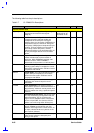
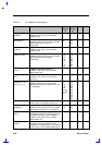
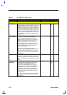
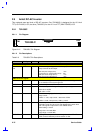
VS2/
CVS2
Voltage Sense 2: This pin is used in
conjunction with VS1 to determine the
operating voltage of the card. This pin is
internally pulled high to the voltage of the
+5V power pin under the combined control
of the external data write bits and the CD
pull up control bits. This pin connects to
PCMCIA socket pin 57.
104 179 I/O 1
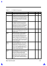
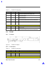
VS1/
CVS1
Voltage Sense 1: This pin is used in
conjunction with VS2 to determine the
operating voltage of the card. This pin is
internally pulled high to the voltage of the
+5V power pin under the combined control
of the external data write bits and the CD
pull up control bits. This pin connects to
PCMCIA socket pin 43.
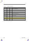
76 152 I/O 1
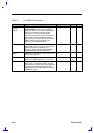
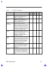
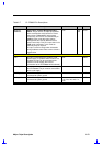
SOCKET
_VCC
Connect these pins to the Vcc supply of the
socket (pins 17 and 51 of the respective
PCMCIA socket). These pins can be 0, 3.3,
or 5 V, depending on card presence, card
type, and system configuration. The socket
interface out puts (listed in this table, Table
2-2) will operate at the voltage applied to
these pins, independent of the voltage
applied to other CL-PD6832 pin groups.
117,
98, 79,
60
200,180
, 160,
143
PW
R