


2-32 Service Guide
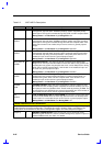
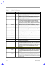
Table 2-3 NM2160 Pin Descriptions
Number Pin name I/O Description
72 FRAME# I/O
Frame This active-low signal is driven by the bus master to
indicate the beginning and duration of an access. NM2160 drives
this pin in the Bus Master mode
65 PAR I/O
Parity Even parity across AD31:0&C/BE3:0# is driven by the bus
master during address and write data phases and driven by
NM2160 during read data phases
67 TRDY# I/O
S/T/S
Target ready This active low signal indicates NM2160’s ability to
complete the current data phase of the transaction. During a read
cycle TRDY# indicates that valid data is present on AD 31:00.
During a write, it indicates NM2160 is prepared to accept data.
Wait states will be inserted until both TRDY#&IRDY# are asserted
together. Input when NM2160 is in Bus Master
68 STOP# I/O
S/T/S
Stop This active low signal indicates that NM2160 is requesting
the master to terminate at the end of current transaction. Input
when NM2160 is in Bus Master
69 DEVSEL# I/O
S/T/S
Device Select This active low signal indicates that NM2160 has
decoded its address as the target of the current access. Input
when NM2160 is in Bus Master
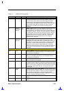
81 IDSEL I
Initialization Device Select This input signal is used as a chip
select during configuration read and write transactions
71 BCLK I
Bus Clock This input provides the timing for all transactions on
PCI bus
66 BREQ# O
T/S
Bus Request This active-low output is used to indicate the arbiter
that NM2160 desires use of the bus
88 BGNT# I
Bus Grant This active-low input indicates NM2160 that access to
the bus has been granted
84 RESET# I
Reset This active-low input is used to initialize NM2160
70 INTA# O
O/D
Interrupt request A This active low “level sensitive” output
indicates an interrupt request
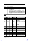
145 CLKRUN# I/O
O/D
Clockrun The master device will control this signal to the NM2160,
according to the Mobile Computing PCI design guide. If this signal
is sampled high by the NM2160 and the PCI clock related
functions are not completed then it will drive this signal Low to
request the Central Clock Resource for the continuation of the PCI
clock. This function can be Enabled/Disabled through register
GR12 bit 5
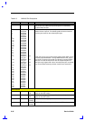
Clock Interface
93 XTAL1/
14MHZ
I
Oscillator Input This pin is used to feed in a reference clock of
14.31818Mhz from an external oscillator OR a Clock Source to the
internal PLL. NM2160 CR70[5] can be programmed to provide a
1Xfsc or 4xfsc NTSC sub-carrier frequency for an external analog
Encoder
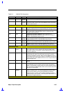
92 XTAL2/
17MHZ
I
Oscillator Input This pin is used to feed in a reference clock of
17.734480Mhz from an external oscillator OR a Clock Source to
the internal PLL. NM2160 CR70[5] can be programmed to provide
a 1Xfsc or 4xfsc PAL/SECAM sub-carrier frequency for an external
Analog Encoder