


2-52 Service Guide
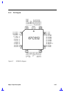
2.6.4 Pin Description
Table 2-6 NS97338VJG Pin Descriptions
Pin No. I/O Description
A15-A0 67, 64,
62-60,
29, 19-
28
I
Address.
These address lines from the microprocessor determine
which internal register is accessed. A0-A15 are don't cares during
DMA transfer.
/ACK 83 I
Parallel Port Acknowledge.
This input is pulsed low by the printer to
indicate that it has received the data from the parallel port. This pin
has a nominal 25 KΩ pull-up resistor attached to it.
ADRATE0,
ADRATE1
96,
46
O
FDD Additional Data Rate 0,1.
These outputs are similar to DRATE0,
1. They are provided in addition to DRATE0, 1. They reflect the
currently selected FDC data rate, (bits 0 and 1 in the Configuration
Control Register (CCR) or the Data Rate Select Register (DSR),
whichever was written to last). ADRATE0 is configured when bit 0 of
ASC is 1. ADRATE1 is configured when bit 4 of ASC is 1. (See IRQ5
and DENSEL for further information).
/AFD 76 I/O
Parallel Port Automatic Feed XT.
When this signal is low, the printer
automatically line feed after printing each line. This pin is in a tristate
condition 10 ns after a 0 is loaded into the corresponding Control
Register bit. The system should pull this pin high using a 4.7 KΩ
resistor.
AEN 18 I
Address Enable.
When this input is high, it disables function selection
via A15-A0. Access during DMA transfer is not affected by this pin.
/ASTRB 79 O
EPP Address Strobe.
This signal is used in EPP mode as address
strobe. It is an active low signal.
BADDR0,
BADDR1
72,
71
I
Base Address.
These bits determine one of the four base addresses
from which the Index and Data Registers are offset. An internal pull-
down resistor of 30 KΩ is on this pin. Use a 10 KΩ resistor to pull this
pin to VCC.
BOUT1,
BOUT2
71,
63
O
UARTs Baud Output.
This multi-function pin supports the associated
serial channel Baud Rate generator output signal if the test mode is
selected in the Power and Test Configuration Register and the DLAB
bit (LCR7) is set. After the Master Reset, this pin offers the SOUT
function.
BUSY 82 I
Parallel Port Busy.
This pin is set high by the printer when it cannot
accept another character. It has a nominal 25 KΩ pull-down resistor
attached to it.
CFG0 63 I
SIO Configuration Strap.
These CMOS inputs select 1 of 4 default
configurations in which the PC97338 powers up. An internal pull-down
resistor of 30 KΩ is on this. Use a 10 KΩ resistor to pull these pins to
VCC. CFG0 is multiplexed with SOUT2, BOUT2 and IRTX.
/CS0,
/CS1
51, 3 O
Programmable Chip Select.
/CS0, 1 are programmable chip select
and/or latch enable and/or output enable signals that can be used as
game port, I/O expand, etc. The decoded address and the assertion
conditions are configured via the 97338VJG’s configuration registers.