


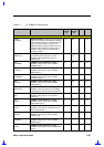
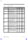

Major Chips Description 2-61
•
An asterisk (*)
at the end of a pin name indicates an active-low signal that is a general-interface
for the CL-PD6832.
•
A double-dagger superscript ( ) at the end of the pin name indicates signals that are used for
power-on configuration switches.
•
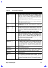
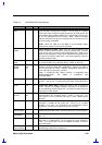
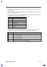
The l/O-type code (I/O) column indicates the input and output configurations of the pins on the
CL-PD6832.The possible types are defined below.
I/O Type Description
I Input pin
I-PU Input pin with internal pull-up resistor
O Constant-driven output pin
I/O Input/output pin
O-OD Open-drain output pin
O-TS Tristate output pin
GND Ground pin
PWR Power pin
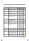
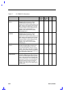
•
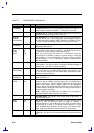
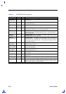
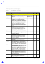
The power-type code (Pwr.) column indicates the output drive power source for an output pin or the pull-
up power source for an input pin on the CL-PD6832. The possible types are defined below.
Power Type Output or Pull-up Power Source
1 +5v: powered from a 5-volt power supply
2 A_SOCKET_VCC: powered from the Socket A Vcc supply connecting to PC Card
pins 17 and 51 of Socket A
3
B_SOCKET_VCC: powered from the Socket B Vcc supply connecting to PC Card
pins 17 and 51 of Socket B
4 PCI_VCC: powered from the PCI bus power supply
5 CORE_VDD: powered from a 3.3-volt power supply