


2-36 Service Guide
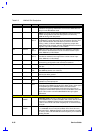
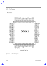
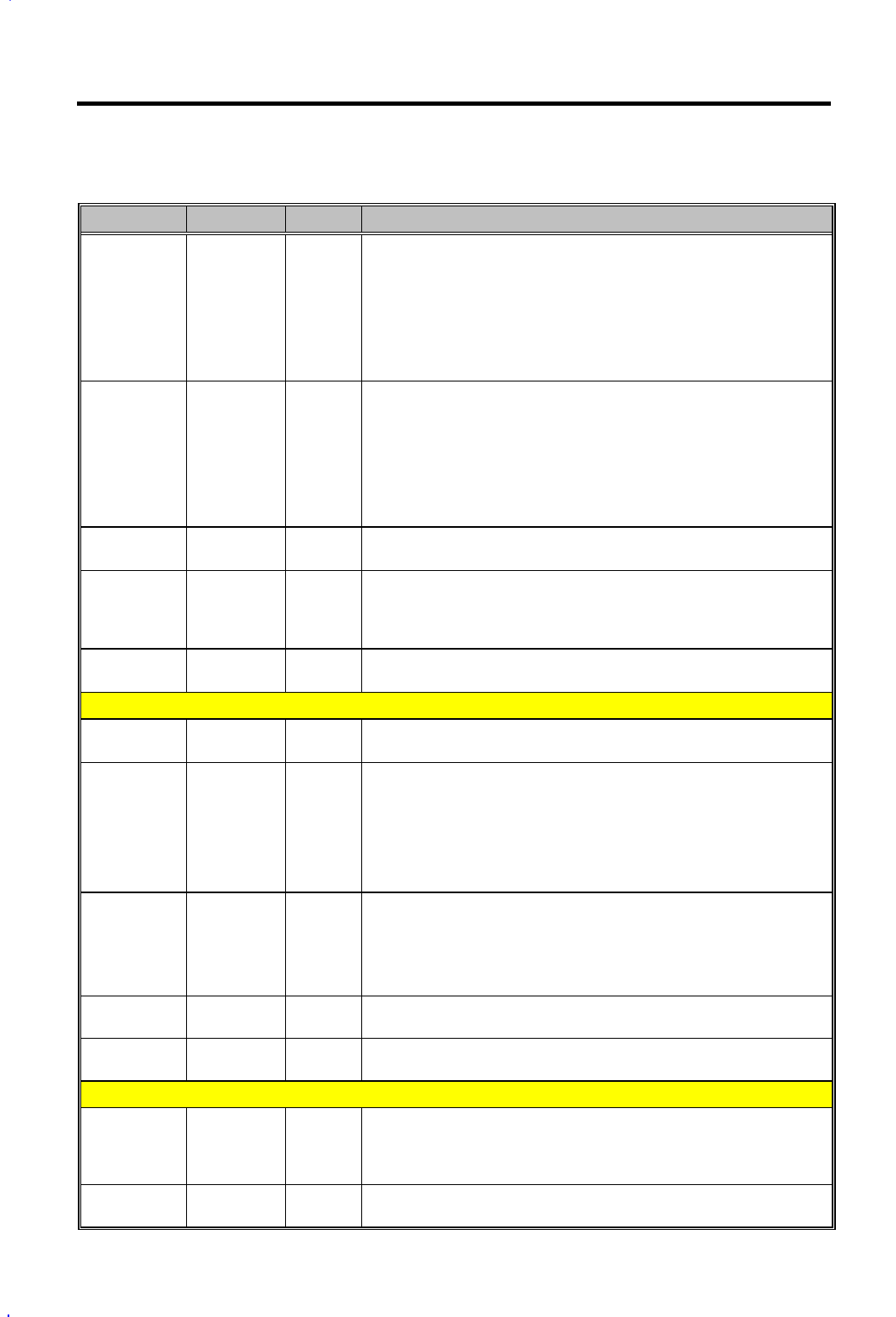
Table 2-3 NM2160 Pin Descriptions
Number Pin name I/O Description
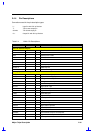
167
166
165
164
163
162
161
160
UV7
UV6
UV5
UV4
UV3
UV2
UV1
UV0
I
Chrominance Data 7:0 These are the 8-bits of chrominance data
that are input to the ZV port of NM2160
159
158
155
152
151
150
149
148
Y7
Y6
Y5
Y4
Y3
Y2
Y1
Y0
I
Luminance Data 7:0 These are the 8-bits of luminance data that
are input to the ZV port of NM2160
144 HREF I
Horizontal Synchronization Pulse: This input signal provides the
horizontal synchronization pulse to the ZV port
168 PCLK I
Video Clock This signal is used to clock the valid video data and
the HREF signal into the ZV Port. The maximum rate is 16 MHz.
During display time, rising edge of PCLK is used to clock the 16-bit
pixel data into the ZV Port
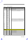
146 VS I
Vertical SYNC This signal supplies the Vertical synchronization
pulse to the ZV Port of NM2160
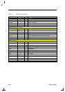
Miscellaneous Pins
87 MTEST# I
Memory test This active low signal is used for internal memory
testing. This should be tied high for normal system operation
145 CLKRUN# I/O
O/D
Clockrun The master device will control this signal to the NM2160,
according to the Mobile computing PCI design guide. If this signal
is sampled high by the NM2160 and the PCI clock related
functions are not completed then it will drive this signal Low to
request the Central Clock Resource for the continuation of the PCI
clock. This function can be Enabled/Disabled through reg. GR12
bit 5
110 VGADIS I
VGA Disable This pin when active disables all the accesses to the
NM2160 controller, but maintains all the screen refreshes. GR12
bit-4 enables/disables this feature.
NOTE: When driven by an external source, the swing on this pin
should not be above LVDD
11 DDC2BD I/O
O/D
DDC Data pin
12 DDC2BC I/O
O/D
DDC Clock pin
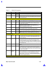
Power pins
10, 29, 44,
59, 80, 114,
125, 138,
153
VSSP Host bus interface ground, ZV interface ground and Panel
Interface ground
23, 64, 109,
88
GND Logic ground