


Stylus C40UX/C40SX/C20UX/C20SX Revision A
Operating Principles Electrical Circuit Operating Principles 42
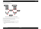
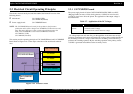
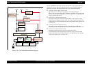
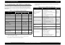
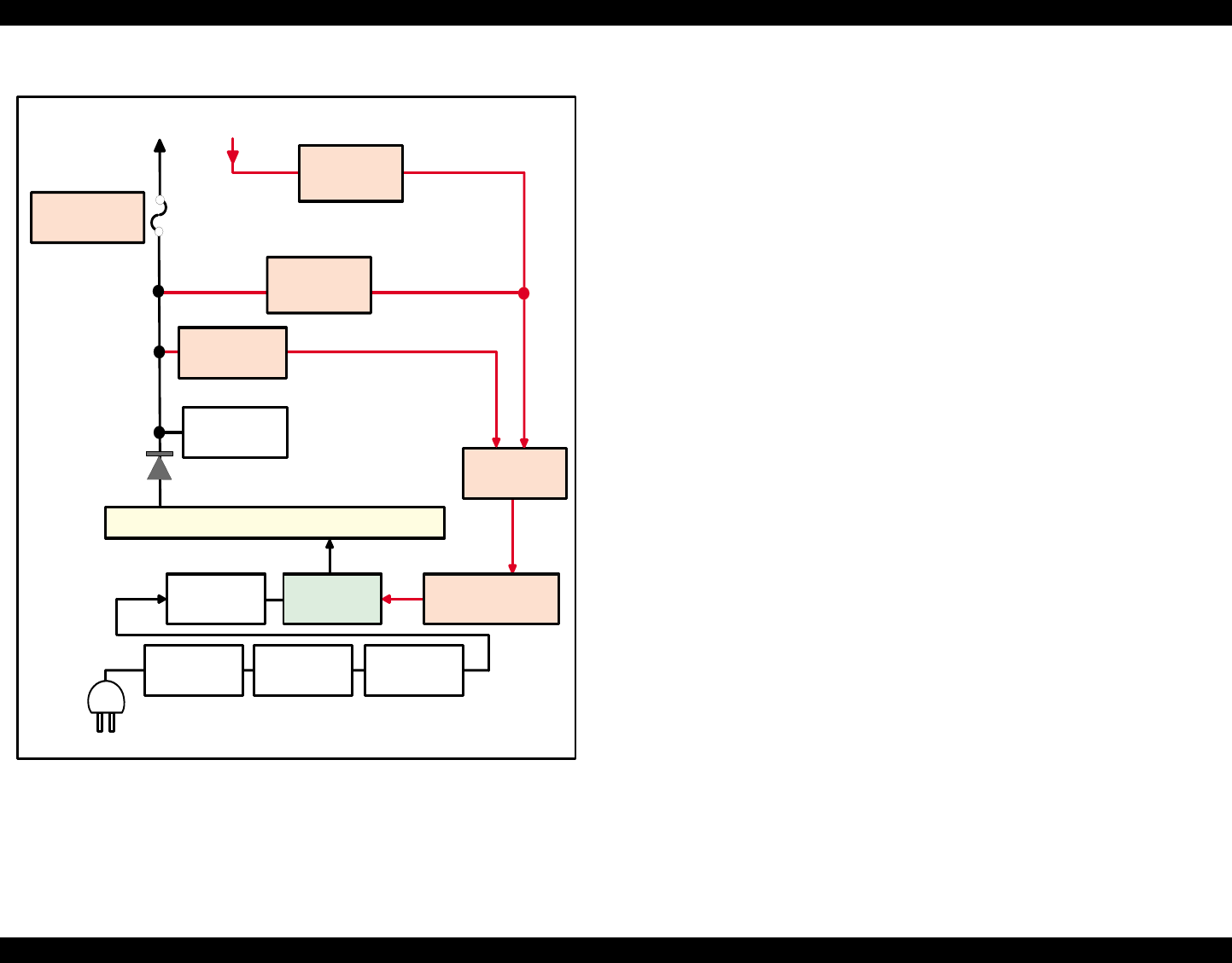
Figure 2-20. C417 PSB/PSE Board Block Diagram
The C417 PSB/PSE board has the various control circuits to stop voltage output if a
malfunction occurs on the power supply board or the main board while the printer
mechanism is on duty. Following explains each control and protection circuit.
+36V line constant voltage control circuit:
The output level of +36V line is monitored by a R92, R93,Q91,ZD51.
When + 36V line reaches about 36.4V, ZD51 has a continuity with and PC1 start
the operation via Q91. Consequently, Q1 switching operation is controlled by this
circuit to stabilize the 36V line.
+36Vline over voltage protection circuit:
The output voltage line is monitored by ZD52,ZD87. If the output level of the
voltage level of +36DC line exceeds +48V, this circuit stops the operation of the
switching FET Q1 via PC1,Q82,Q83 and prevents high voltage from applied to the
secondary side
+36Vline over current protection circuit:
The output voltage is monitored by the F51. When the abnormal current is
detected by F51, F51 is fused and cut off the +36V line output to the Main board
+5V line over voltage protection circuit:
The output voltage level of the +5V line is monitored by ZD53.
If the output level of the voltage level of +5DC line exceeds +7V, this circuit
stops the operation of the switching FET Q1 via PC1,Q82,Q83and prevents high
voltage from applied to the secondary side.
+36VDC over
current protection
+5VDC line
over voltage
limitation
+36VDC line
over voltage
limitation
+36VDC Line
Constant Control
Smoothing
Circuit
Photo
Coupler
TRANS(T1)
Feed back circuit
Main
Switching
Smoothing
Circuit
Over Current
Protection
Filter Circuit
Full Wave
rectifier circuit
+5VDC+36VDC
F51
ZD53
ZD52,87
ZD51,R92,93,Q91
C51
PC1