


Chapter 3 Hardware Overview
6023E/6024E/6025E User Manual 3-6 ni.com
The approximately 4 V step from 4 V to 1 mV is 4,000% of the new
full-scale range. It can take as long as 100 µs for the circuitry to settle to
1 LSB after such a large transition. In general, this extra settling time is not
needed when the PGIA is switching to a lower gain.
Settling times can also increase when scanning high-impedance signals
due to a phenomenon called charge injection, where the analog input
multiplexer injects a small amount of charge into each signal source when
that source is selected. If the impedance of the source is not low enough,
the effect of the charge—a voltage error—has not decayed by the time the
ADC samples the signal. For this reason, keep source impedances under
1kΩ to perform high-speed scanning.
Due to the previously described limitations of settling times resulting from
these conditions, multiple-channel scanning is not recommended unless
sampling rates are low enough or it is necessary to sample several signals
as nearly simultaneously as possible. The data is much more accurate and
channel-to-channel independent if you acquire data from each channel
independently (for example, 100 points from channel 0, then 100 points
from channel 1, then 100 points from channel 2, and so on).
Analog Output
♦ 6025E and 6024E only
These devices supply two channels of analog output voltage at the I/O
connector. The bipolar range is fixed at ±10 V. Data written to the
digital-to-analog converter (DAC) is interpreted in two’s complement
format.
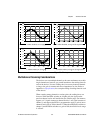
Analog Output Glitch
In normal operation, a DAC output glitches whenever it is updated with a
new value. The glitch energy differs from code to code and appears as
distortion in the frequency spectrum.