


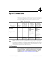
Chapter 3 Hardware Overview
© National Instruments Corporation 3-9 6023E/6024E/6025E User Manual
scheme reduces the need to change physical connections to the I/O
connector for different applications.
You can also individually enable each of the PFI pins to output a specific
internal timing signal. For example, if you need the UPDATE* signal as an
output on the I/O connector, software can turn on the output driver for the
PFI5/UPDATE* pin.
Device and RTSI Clocks
♦ PCIandPXIbuses
Many device functions require a frequency timebase to generate the
necessary timing signals for controlling A/D conversions, DAC updates,
or general-purpose signals at the I/O connector.
These devices can use either its internal 20 MHz timebase or a timebase
received over the RTSI bus. In addition, if you configure the device to use
the internal timebase, you can also program the device to drive its internal
timebase over the RTSI bus to another device thatis programmed to receive
this timebase signal. This clock source, whether local or from the RTSI bus,
is used directly by the device as the primary frequency source. The default
configuration at startup is to use the internal timebase without driving the
RTSI bus timebase signal. This timebase is software selectable.
♦ PXI-6025E
The RTSI clock connects to other devices through the PXI trigger bus on
the PXI backplane. The RTSI clock signal uses the PXI trigger <7> line for
this connection.
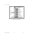
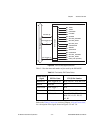
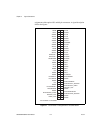
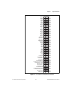
RTSI Triggers
♦ PCIandPXIbuses
The seven RTSI trigger lines on the RTSI bus provide a very flexible
interconnection scheme for any device sharing the RTSI bus. These
bidirectional lines can drive any of eight timing signals onto the RTSI bus
and can receive any of these timing signals. This signal connection scheme
is shown in Figure 3-5 for PCI devices and Figure 3-6 for PXI devices.