


Chapter 4 Signal Connections
6023E/6024E/6025E User Manual 4-4 ni.com
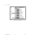
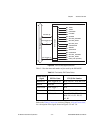
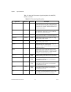
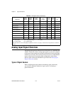
Table 4-2 shows the I/O connector signal descriptions for the 6023E,
6024E, and 6025E.
Table 4-2. I/O Connector Signal Descriptions
Signal Name Reference Direction Description
AIGND — — Analog inputground—these pinsare thereference pointfor
single-ended measurements in RSE configuration and the
bias current return point for DIFF measurements. All three
ground references—AIGND, AOGND, and DGND—are
connected on your device.
ACH<0..15> AIGND Input Analog input channels 0 through 15—you can configure
each channel pair, ACH<i, i+8> (i = 0..7), as either one
DIFF input or two single-ended inputs.
AISENSE AIGND Input Analog input sense—this pin serves as the reference node
for any of channels ACH <0..15> in NRSE configuration.
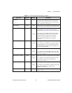
DAC0OUT
1
AOGND Output Analog channel 0 output—this pin supplies the voltage
output of analog output channel 0.
DAC1OUT
1
AOGND Output Analog channel 1 output—this pin supplies the voltage
output of analog output channel 1.
AOGND — — Analog output ground—the analog output voltages are
referenced to this node. All three ground
references—AIGND,AOGND,andDGND—areconnected
together on your device.
DGND — — Digital ground—this pin supplies the reference for the
digital signals at the I/O connector as well as the +5 VDC
supply.All three ground references—AIGND, AOGND,
and DGND—are connected on your device.
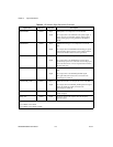
DIO<0..7> DGND Input or
Output
Digital I/O signals—DIO6 and 7 can control the up/down
signal of general-purpose counters 0 and 1, respectively.
PA<0 .. 7>
2
DGND Input or
Output
Port A bidirectional digital data lines for the 82C55A
programmable peripheral interface on the 6025E. PA7
is the MSB. PA0 is the LSB.
PB<0..7>
2
DGND Input or
Output
Port B bidirectional digital data lines for the 82C55A
programmable peripheral interface on the 6025E. PB7
is the MSB. PB0 is the LSB.
PC<0..7>
2
DGND Input or
Output
Port C bidirectional digital data lines for the 82C55A
programmable peripheral interface on the 6025E. PC7
is the MSB. PC0 is the LSB.
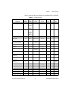
+5 V DGND Output +5 VDC Source—these pins are fused for up to 1 A of
+5 V supply on the PCI and PXI devices, or up to 0.75 A
from a DAQCard device. The fuse is self-resetting.