


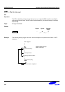
S3C8275X/F8275X/C8278X/F8278X/C8274X/F8274X CLOCK CIRCUIT
7-5
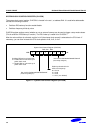
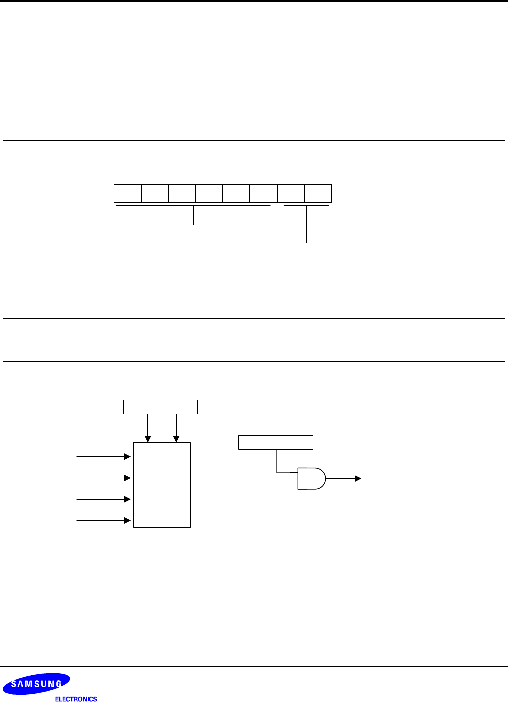
CLOCK OUTPUT CONTROL REGISTER (CLOCON)
The clock output control register, CLOCON, is located in set 1 bank 1, at address E8H. It is read/write
addressable and has the following functions:
• Clock output frequency selection
After a reset, fxx/64 is select for clock output frequency because the reset value of CLOCON.1−.0 is "00b".
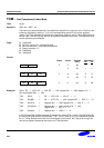
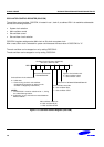
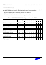
Clock Output Control Register (CLOCON)
E8H, Set 1, Bank 1, R/W
LSBMSB .7 .6 .5 .4 .3 .2 .1 .0
Not used for S3C8275X/C8278X/C8274X
(must keep always "0")
Clock output frequency selection bits:
00 = Select fxx/64
01 = Select fxx/16
10 = Select fxx/8
11 = Select fxx/4
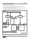
Figure 7-8. Clock Output Control Register (CLOCON)
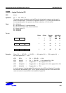
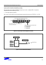
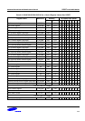
MUX
fxx/64
fxx/16
fxx/8
fxx/4
P0CONH.5-.4
CLOCON.1-.0
CLKOUT/P0.6
Figure 7-9. Clock Output Block Diagram