


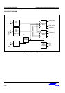
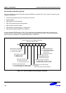
LCD CONTROLLER/DRIVER S3C8275X/F8275X/C8278X/F8278X/C8274X/F8274X
13-6
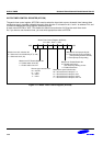
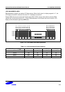
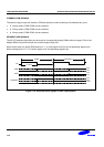
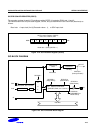
COMMON (COM) SIGNALS
The common signal output pin selection (COM pin selection) varies according to the selected duty cycle.
• In 1/4 duty mode, COM0-COM3 pins are selected
• In 1/3 duty mode, COM0-COM2 pins are selected
• In 1/2 duty mode, COM0-COM1 pins are selected
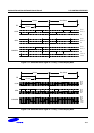
SEGMENT (SEG) SIGNALS
The 32 LCD segment signal pins are connected to corresponding display RAM locations at page 2. Bits of the
display RAM are synchronized with the common signal output pins.
When the bit value of a display RAM location is "1", a select signal is sent to the corresponding segment pin.
When the display bit is "0", a 'no-select' signal to the corresponding segment pin.
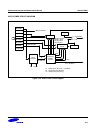
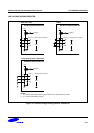
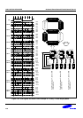
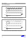
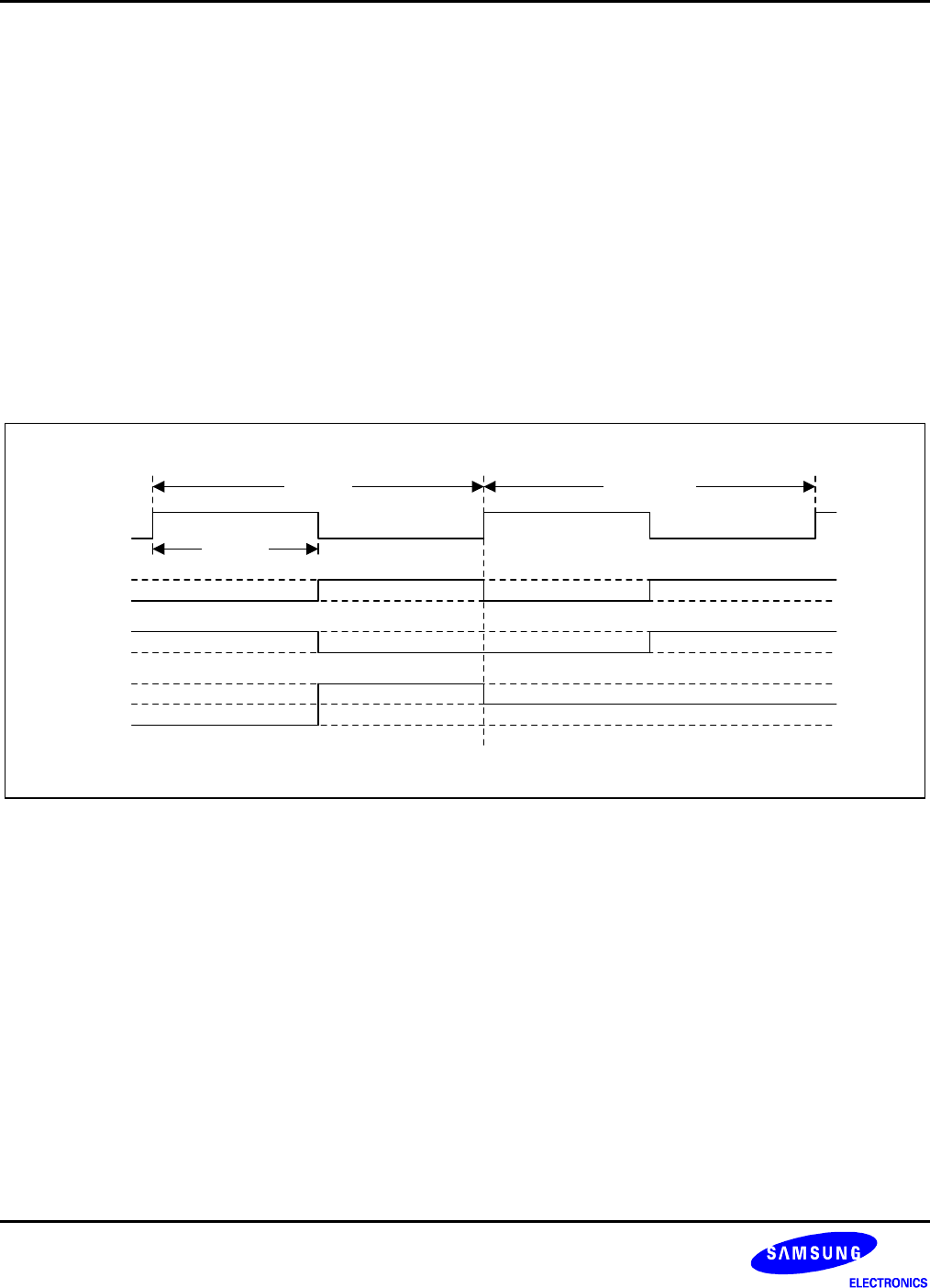
1 Frame
Select Non-Select
FR
COM
SEG
COM-SEG
V
LC0
V
SS
V
LC0
V
SS
V
LC0
V
SS
-V
LC0
Figure 13-6. Select/No-Select Signals in Static Display Mode