


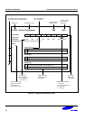
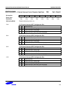
CONTROL REGISTERS S3C8275X/F8275X/C8278X/F8278X/C8274X/F8274X
4-4
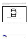
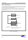
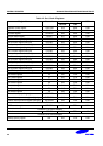
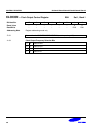
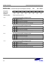
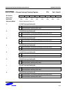
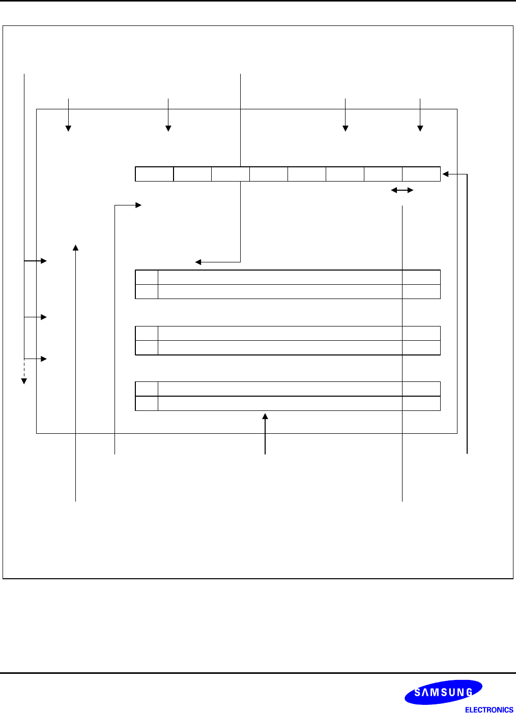
FLAGS - System Flags Register
.7 Carry Flag (C)
.6 Zero Flag (Z)
.5
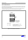
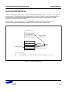
Bit Identifier
Reset Value
Read/Write
Bit Addressing
Mode
R = Read-only
W = Write-only
R/W = Read/write
'-' = Not used
Type of addressing
that must be used to
address the bit
(1-bit, 4-bit, or 8-bit)
nRESET value notation:
'-' = Not used
'x' = Undetermined value
'0' = Logic zero
'1' = Logic one
Bit number(s) that is/are appended to
the register name for bit addressing
Name of individual
bit or related bits
Full Register nameRegister ID
Sign Flag (S)
0
Operation does not generate a carry or borrow condition
1
Operation generates carry-out or borrow into high-order bit 7
0
Operation result is a non-zero value
1
Operation result is zero
0
Operation generates positive number (MSB = "0")
1
Operation generates negative number (MSB = "1")
Description of the
effect of specific
bit settings
Set 1
Register location
in the internal
register file
D5H
Register address
(hexadecimal)
.7 .6 .5
xxx
R/W R/W R/W
Register addressing mode only
.4 .3 .2 .1 .0
x
R/W
x
R/W
x
R/W
x
R/W
0
R/W
Bit number:
MSB = Bit 7
LSB = Bit 0
Figure 4-1. Register Description Format