S3C8275X/F8275X/C8278X/F8278X/C8274X/F8274X ADDRESS SPACES
2-3
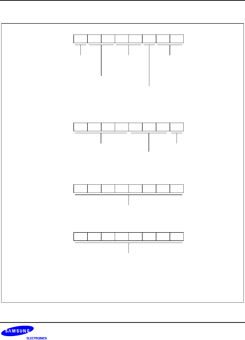
SMART OPTION
ROM Address: 003EH
LSBMSB .7 .6 .5 .4 .3 .2 .1 .0
ISP reset vector change enable/disable bit:
0 = OBP reset vector address
1 = Normal vector (address 0100H)
NOTES:
1. After selecting ISP reset vector address in selecting ISP protection size, don't select upper than ISP
area size.
2. When any values are written in the Smart Option area (003CH-003FH) by LDC instruction, the data of
the area may be changed but the Smart Option is not affected. The data for Smart Option should be
written in the Smart Option area (003CH-003FH) by OTP/MTP tools (SPW2 plus single
programmer, or GW-PRO2 gang programmer).
ISP reset vector address selection bit:
00 = 200H (ISP area size: 256 byte)
01 = 300H (ISP area size: 512 byte)
10 = 500H (ISP area size: 1024 byte)
11 = 900H (ISP area size: 2048 byte)
ISP protection size selection:
(note)
00 = 256 bytes
01 = 512 bytes
10 = 1024 bytes
11 = 2048 bytes
Not used
ISP protection enable/disable bit:
0 = Enable (not erasable by LDC)
1 = Disable (erasable by LDC)
ROM Address: 003FH
LSBMSB .7 .6 .5 .4 .3 .2 .1 .0
Not used
LVR enable/disable bit
(criteria voltage: 2.2V):
0 = Disable LVR
1 = Enable LVR
ROM Address: 003CH
LSBMSB .7 .6 .5 .4 .3 .2 .1 .0
Not used
ROM Address: 003DH
LSBMSB .7 .6 .5 .4 .3 .2 .1 .0
Not used
These bits should be
always logic "110b".
Figure 2-2. Smart Option


