


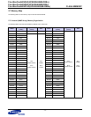


Flex-MuxOneNAND4G(KFM4GH6Q4M-DEBx)
- 10 -
FLASH MEMORY
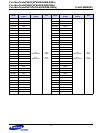
Flex-MuxOneNAND8G(KFN8GH6Q4M-DEBx)
Flex-MuxOneNAND16G(KFKAGH6Q4M-DEBx)
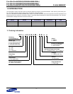
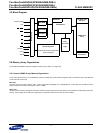
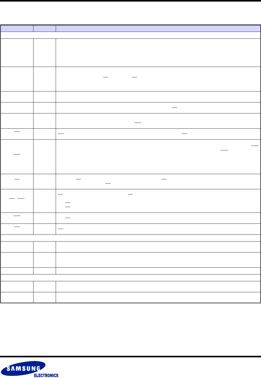
2.4 Pin Description
NOTE :
Do not leave power supply(Vcc-Core/Vcc-IO, VSS) disconnected.
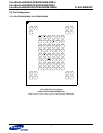
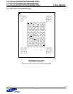
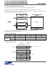
Pin Name Type Nameand Description
Host Interface
ADQ15~ADQ0 I/O
Multiplexed Address/Data bus
- Inputs for addresses during read operation, which are for addressing BufferRAM & Register.
- Inputs data during program and commands for all operations, outputs data during memory array/
register read cycles.
Data pins float to high-impedance when the chip is deselected or outputs are disabled.
INT / INT1 O
Interrupt
Notifies the Host when a command is completed. After power-up, it is at hi-z condition. Once IOBE is set to 1, it does not float
to hi-z condition even when CE
is disabled or OE is disabled. Especially, only when reset(Cold, Warm, Hot, NAND Flash
Core) command in DDP are issued, it operates as open drain output with internal resistor (~50Kohm). The INT is the interrupt
for Single or DDP device. The INT1 is the interrupt for the first DDP device(KFN8GH6Q4M) in QDP(KFKAGH6Q4M)
INT2 O
Interrupt
The INT2 is the interrupt for the second DDP device(KFN8GH6Q4M) in QDP(KFKAGH6Q4M)
RDY O
Ready
Indicates data valid in synchronous read modes and is activated while CE
is low
CLK I
Clock
CLK synchronizes the device to the system bus frequency in synchronous read mode.
The first rising edge of CLK in conjunction with AVD
low latches address input.
WE
I
Write Enable
WE
controls writes to the bufferRAM and registers. Datas are latched on the WE pulse’s rising edge
AVD
I
Address Valid Detect
Indicates valid address presence on address inputs. During asynchronous read operation, all addresses are valid while AVD
is low, and during synchronous read operation, all addresses are latched on CLK’s rising edge while AVD is held low for one
clock cycle.
> Low : for asynchronous mode, indicates valid address; for burst mode, causes starting address to be latched on rising edge
on CLK
> High : device ignores address inputs
RP
I
Reset Pin
When low, RP resets internal operation of Flex-MuxOneNAND. RP status is do not care during power-up
and bootloading. When high, RP
level must be equivalent to Vcc-IO / Vccq level.
CE
/ CE1 I
Chip Enable
CE
-low activates internal control logic, and CE-high deselects the device, places it in standby state,
and places DQ in Hi-Z.
The CE
input enables device for Single or DDP .
The CE
1 input enables the first DDP device(KFN8GH6Q4M) in QDP(KFKAGH6Q4M)
CE2
I
Chip Enable
The CE
2 input enables the second DDP device(KFN8GH6Q4M) in QDP(KFKAGH6Q4M)
OE
I
Output Enable
OE
-low enables the device’s output data buffers during a read cycle.
Power Supply
VCC-Core
/ Vcc
Power for Flex-MuxOneNAND Core
This is the power supply for Flex-MuxOneNAND Core.
VCC-IO
/ Vccq
Power for Flex-MuxOneNAND I/O
This is the power supply for Flex-MuxOneNAND I/O
Vcc-IO / Vccq is internally separated from Vcc-Core / Vcc.
VSS Ground for Flex-MuxOneNAND
etc.
DNU
Do Not Use
Leave it disconnected. These pins are used for testing.
NC
No Connection
Lead is not internally connected.