


Flex-MuxOneNAND4G(KFM4GH6Q4M-DEBx)
- 95 -
FLASH MEMORY
Flex-MuxOneNAND8G(KFN8GH6Q4M-DEBx)
Flex-MuxOneNAND16G(KFKAGH6Q4M-DEBx)
3.13.2 OTP Block Program Operation
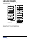
An OTP Block Program Operation accesses the OTP area and programs content from the DataRAM on-chip buffer to the designated page(s)
of the OTP.
A memory location in the OTP area can be programmed only one time (no erase operation permitted).
The OTP area is programmed using the same sequence as normal program operation after being accessed by the command (see section 3.9
for more information).
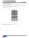
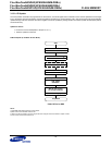
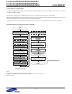
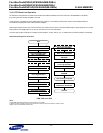
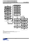
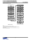
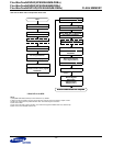
Programming the OTP Area
Issue the OTP Access Command
Write data into the DataRAM (data can be input at anytime between the "Start" and "Write Program commands".
Issue a Flash Block Address (FBA) which is 0000h of NAND Flash Array address map.
Issue a Program command to program the data from the DataRAM into the OTP
When the OTP Block programming is complete,
do a Cold-, Warm-, Hot-, NAND Flash Core Reset to exit the OTP Access mode.