


Flex-MuxOneNAND4G(KFM4GH6Q4M-DEBx)
- 88 -
FLASH MEMORY
Flex-MuxOneNAND8G(KFN8GH6Q4M-DEBx)
Flex-MuxOneNAND16G(KFKAGH6Q4M-DEBx)
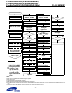
3.12.1.2 PI Block Erase
The PI Block Erase Operation erases the entire PI block including Partition Information. PI Block Access mode entry must be done before
issuing Erase operation for PI Block.
Erasing the PI Area
Issue the PI Access Command(Refer to Chapter 3.12.1.1).
Issue an Erase command to erase the PI area.
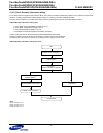
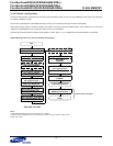
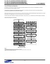
PI Block Erase Operation Flow Chart (In PI Block Access Mode)
NOTE :
1) FBA(NAND Flash Block Address) must be 0000h.
2) ‘Write 0 to interrupt register’ step may be ignored when using INT auto mode. Refer to chapter 2.8.18.1
Start
PI Erase Complete
Write Erase command
DQ=0094h
Wait for INT register
low to high transition
Add: F241h DQ[15]=INT
Add: F220h
Write 0 to interrupt register
2)
Add: F241h DQ=0000h
NO
* DBS, DFS is for DDP
Read Controller
Status Register
Add: F240h
DQ[10]=1(Error)
YES
Write ‘FBA’ of Flash
Add: F100h DQ=FBA
1)
PI Erase Error