


Flex-MuxOneNAND4G(KFM4GH6Q4M-DEBx)
- 68 -
FLASH MEMORY
Flex-MuxOneNAND8G(KFN8GH6Q4M-DEBx)
Flex-MuxOneNAND16G(KFKAGH6Q4M-DEBx)
3.7 Read Operation
See Timing Diagrams 6.1,6.2, 6.3 and 6.4.
The device has two read modes; Asynchronous Read and Synchronous Burst Read.
The initial state machine automatically sets the device into the Asynchronous Read Mode (RM=0) to prevent the spurious altering of memory
content upon device power up or after a Hardware reset. No commands are required to retrieve data in Asynchronous Read Mode.
The Synchronous Read Mode is enabled by setting RM bit of System Configuration1 Register (F221h) to Synchronous Read Mode (RM=1).
See section 2.8.19 for more information about System Configuration1 Register.
3.7.1 Asynchronous Read Mode Operation (RM=0, WM=0)
See Timing Diagrams 6.3 and 6.4
In an Asynchronous Read Mode, data is output with respect to a logic input, AVD
.
Output data will appear on DQ15-DQ0 when a valid address is asserted on A15-A0 while driving AVD
and CE to VIL. WE is held at VIH. The
function of the AVD
signal is to latch the valid address.
Address access time from AVD
low (tAA) is equal to the delay from valid addresses to valid output data.
The Chip Enable access time (tCE) is equal to the delay from the falling edge of CE
to valid data at the outputs.
The Output Enable access time (tOE) is the delay from the falling edge of OE
to valid data at the output.
3.7.2 Synchronous Read Mode Operation (RM=1, WM=X)
See Timing Diagrams 6.1and 6.2
In a Synchronous Read Mode, data is output with respect to a clock input.
The device is capable of a continuous linear burst operation and a fixed-length linear burst operation of a preset length. Burst address
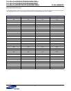
sequences for continuous and fixed-length burst operations are shown in the table below.
Burst Address Sequences
In the burst mode, the initial word will be output asynchronously, regardless of BRWL. While the following words will be determined by BRWL
value.
The latency is determined by the host based on the BRWL bit setting in the System Configuration 1 Register. The default BRWL is 4 latency
cycles. At clock frequencies of 40MHz or lower, latency cycles can be reduced to 3. BRWL can be set up to 7 latency cycles.
The BRWL registers in System Configuration 1 Register can be read during a burst read mode by using the AVD
signal with the address
F221h.
Start
Addr.
Burst Address Sequence(Decimal)
Continuous Burst 4-word Burst 8-word Burst 16-word Burst 32-word Burst
Wrap
around
0 0-1-2-3-4-5-6... 0-1-2-3-0... 0-1-2-3-4-5-6-7-0... 0-1-2-3-4-....-13-14-15-0... 0-1-2-3-4-....-29-30-31-0...
1 1-2-3-4-5-6-7... 1-2-3-0-1... 1-2-3-4-5-6-7-0-1... 1-2-3-4-5-....-14-15-0-1... 1-2-3-4-5-....-30-31-0-1...
2 2-3-4-5-6-7-8... 2-3-0-1-2... 2-3-4-5-6-7-0-1-2... 2-3-4-5-6-....-15-0-1-2... 2-3-4-5-6-....-31-0-1-2...
.
.
.
.
.
.
.
.
.
.
.
.