


Flex-MuxOneNAND4G(KFM4GH6Q4M-DEBx)
- 82 -
FLASH MEMORY
Flex-MuxOneNAND8G(KFN8GH6Q4M-DEBx)
Flex-MuxOneNAND16G(KFKAGH6Q4M-DEBx)
3.11 Erase Operation
3.11.1 Block Erase Operation
See Timing Diagram 6.14
The device can be erased one block at a time. To erase a block is to write all 1's into the desired memory block by executing the Internal Erase
Routine. All previous data is lost.
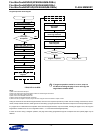
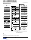
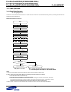
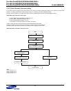
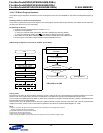
Block Erase Operation Flow Chart
NOTE :
1) ‘Write 0 to interrupt register’ step may be ignored when using INT auto mode. Refer to chapter 2.8.18.1
In order to perform the Internal Erase Routine, the following command sequence is necessary.
The Host selects Flash Core of DDP chip.
The Host sets the block address of the memory location.
The Erase Command initiates the Internal Erase Routine. During the execution of the Routine, the host is
not required to provide further controls or timings. During the Internal erase routine, all commands, except
the Reset command and Erase Suspend Command, written to the device will be ignored.
A reset or power off during an erase operation will cause data corruption at the corresponding location Block.
Start
Write ‘DFS*, FBA’ of Flash
Add: F100h DQ=DFS*, FBA
Write ‘Erase’ Command
Add: F220h DQ=0094h
Wait for INT register
Add: F241h DQ=[15]=INT
low to high transition
: If erase operation results in an error, map out
the failing block and replace it with another block.
*
Write 0 to interrupt register
1)
Add: F241h DQ=0000h
* DBS, DFS is for DDP
Select DataRAM for DDP
Add: F101h DQ=DBS*
Add: F240h DQ[10]=Error
Erase completed
DQ[10]=0?
YES
Erase Error
NO
Read Controller
Status Register
Read Write Protection Status
Add: F24Eh DQ=US,LS,LTS