


Flex-MuxOneNAND4G(KFM4GH6Q4M-DEBx)
- 77 -
FLASH MEMORY
Flex-MuxOneNAND8G(KFN8GH6Q4M-DEBx)
Flex-MuxOneNAND16G(KFKAGH6Q4M-DEBx)
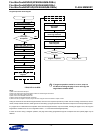
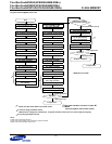
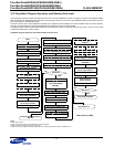
3.9.1 Cache Program Operation
See Timing Diagram 6.12
The Cache Program is to enhance the performance of Program Operation. Employing Cache Program operation, transfer time from Host to
DataRAM can be shadowed, therefore write performance will increase.
In Cache Program, since 4KB data is to be programmed into NAND Flash Array in another advanced way.
1. 4KB Data write from host to DataRAMs.
2. Cache Program command issue. This will turn INT pin to busy state
1)
, OnGo bit sets to ‘1’.
(Note that before issuing ‘Cache Program Command’, host should make sure that the target blocks are unlocked.)
3. 4KB data will be sequentially transferred to a page buffer in NAND Flash Array.
4. When this transfer operation is complete, programming into NAND Flash Array will automatically start, and at the same time, INT bit will turn
to ‘1’ to indicate that DataRAMs are now ready to be written with next 4KB data.
5. When second 4KB is written to two DataRAMs, another Cache Program command is issued and INT bit will go to ‘0’
1)
.
If host wants to program data less than 8 sectors, unwanted area to be programmed must be written to all ‘1’s.
When INT bit goes to ‘1’ after second data transfer from DataRAMs to Page Buffers are complete, user may check the Status Register to
check the Cache program status. During Cache Program, Error bit shows the status of previous program operation.
For the final 4KB program of Cache Program scheme, host should issue Program Command(0080h). And when the final page is programmed,
INT bit will turn to ‘1’ and OnGo status bit - which indicates the overall Cache Program ongoing status - will go to ‘0’. At the completion of
Cache Program operation, Error bit will show the pass/fail status overall status of program, and previous ~ current bit will show where the error
occurred accordingly (Refer to the below diagram.)
Note that Cache Program command cannot be performed on OTP block and 1st block OTP.
Cache Program operation must be utilized within a same area partitioned as SLC or MLC.
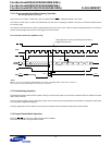
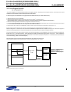
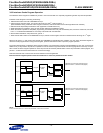
NOTE :
2 and 2’ are concurrent; 3 and 3’ are concurrent
Page A
3’) Program
Sector0
Sector7
DataRAM1
DataRAM0
Page Buffer
(4 KB)
2’) Copy to
Page Buffer
1) Write to DataRAM (Page A)
Page B
2) Wait for INT bit = 1
3) Write to DataRAM (Page B)
4 KB