


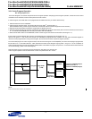
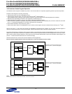
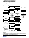

Flex-MuxOneNAND4G(KFM4GH6Q4M-DEBx)
- 81 -
FLASH MEMORY
Flex-MuxOneNAND8G(KFN8GH6Q4M-DEBx)
Flex-MuxOneNAND16G(KFKAGH6Q4M-DEBx)
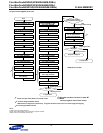
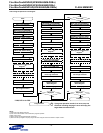
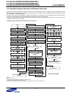
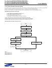
3.10 Copy-Back Program Operation with Random Data Input
The Copy-Back Program Operation with Random Data Input in Flex-MuxOneNAND consists of 3 phases, Load data into DataRAM, Modify
data and program into designated page. Data from the source page is saved in one of the on-chip DataRAM buffers and modified by the host,
then programmed into the destination page.
As shown in the flow chart, data modification is possible upon completion of load operation. ECC is also available at the end of load operation.
Therefore, using hardware ECC of Flex-MuxOneNAND, accumulation of 4 bit error can be avoided.
Copy-Back Program Operation with Random Data Input will be effectively utilized at modifying certain bit, byte, word, or sector of source page
to destination page while it is being copied.
Copy-Back Program Operation with Random Data Input Flow Chart
NOTE :
1) BSA must be 1000.
2) FSA must be 00 and BSC must be 000 within program operation.
3) Writing System Configuration Register is optional.
4) ‘Write 0 to interrupt register’ step may be ignored when using INT auto mode. Refer to chapter 2.8.18.1
Start
Write ‘DFS*, FBA’ of Flash
Add: F100h DQ=DFS, FBA
Write ‘FPA, FSA’ of Flash
Add: F107h DQ=FPA, FSA
Select DataRAM for DDP
Add: F101h DQ=DBS
* DBS, DFS is for DDP
Wait for INT register
low to high transition
Add: F241h DQ[15]=INT
Random Data Input
Write ‘DFS, FBA’ of Flash
Add: F100h DQ=DFS, FBA
Write ‘FPA, FSA’ of Flash
Add: F107h DQ=FPA, FSA
2)
Write ‘Program’ Command
Add: F220h
DQ=0080h
Write 0 to interrupt register
4)
Add: F241h DQ=0000h
Add: Random Address in
Selected DataRAM
DQ=Data
Copy back completed
Read Controller
Status Register
Add: F240h DQ[10]=Error
DQ[10]=0?
Copy back Error
YES
NO
Write ‘BSA
1)
, BSC’ of DataRAM
Add: F200h DQ=0800h
2)
Write ‘Load’ Command
Add: F220h DQ=0000h
Wait for INT register
low to high transition
Add: F241h DQ[15]=INT
Write 0 to interrupt register
4)
Add: F241h DQ=0000h
DQ[10]=0?
YES
NO
Map Out
Write ‘BSA
1)
, BSC’ of DataRAM
Add: F200h DQ=0800h
2)
Read Write Protection Status
Add: F24Eh DQ=US,LS,LTS
Write System Configuration
Add: F221h DQ=ECC
Register
3)
Read ECC Status Register1
Add: FF00h DQ=ER1[12:8], ER0[4:0]
Read ECC Status Register2
Add: FF01h DQ=ER3[12:8], ER2[4:0]
Read ECC Status Register3
Add: FF02h DQ=ER5[12:8], ER4[4:0]
Read ECC Status Register4
Add: FF03h DQ=ER7[12:8], ER6[4:0]
Write System Configuration
Add: F221h DQ=ECC
Register
3)