


Flex-MuxOneNAND4G(KFM4GH6Q4M-DEBx)
- 100 -
FLASH MEMORY
Flex-MuxOneNAND8G(KFN8GH6Q4M-DEBx)
Flex-MuxOneNAND16G(KFKAGH6Q4M-DEBx)
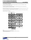
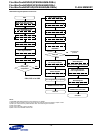
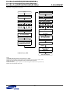
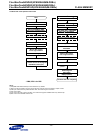
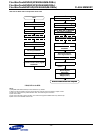
1st Block OTP Lock Operation Flow Chart
NOTE :
1) FBA(NAND Flash Block Address) could be omitted or any address.
2) ‘Write 0 to interrupt register’ step may be ignored when using INT auto mode. Refer to chapter 2.8.18.1
3) Data input could be done anywhere between "Start" and "Write Program Command".
4) FBA must be 0000.
5) FSA must be 00 within program operation. The 0196h is the page49 of NAND Flash Array address map.
6) BSA must be 1000 and BSC must be 000.
Start
Write Data into DataRAM
3)
Add: 1st Word
DQ=XXF3h(Locking bit)
in sector4 of main of the page49
Write ‘OTP Access’ Command
Add: F220h DQ=0065h
Wait for INT register
Add: F241h DQ[15]=INT
low to high transition
Write 0 to interrupt register
2)
Add: F241h DQ=0000h
Write ‘DFS, FBA’ of Flash
1)
Add: F100h DQ=DFS, FBA
Select DataRAM for DDP
Add: F101h DQ=0000h(DBS*)
* DBS, DFS is for DDP
Write ‘FPA, FSA’ of Flash
Add: F107h DQ=0196h
5)
Write ‘BSA, BSC’ of DataRAM
Add: F200h DQ=0800h
6)
Write Program command
DQ=0080h
Wait for INT register
low to high transition
Add: F241h DQ[15]=INT
Add: F220h
Write 0 to interrupt register
2)
Add: F241h DQ=0000h
Automatically
updated
Update Controller
Add: F240h
Status Register
1st Block OTP lock completed
DQ[5]=1(OTP
BL)
Write ‘FBA’ of Flash
Add: F100h DQ=FBA
4)
Do Cold reset