


Flex-MuxOneNAND4G(KFM4GH6Q4M-DEBx)
- 58 -
FLASH MEMORY
Flex-MuxOneNAND8G(KFN8GH6Q4M-DEBx)
Flex-MuxOneNAND16G(KFKAGH6Q4M-DEBx)
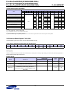
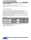
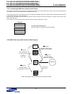
3.3 Reset Mode Operation
The Flex-MuxOneNAND has 4 reset modes: Cold/Warm/Hot Reset, and NAND Flash Array Reset. Section 3.3 discusses the operation of
these reset modes.
The Register Reset Table shows the which registers are affected by the various types of Reset operations.
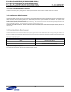
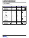
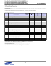
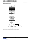
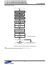
Internal Register Reset Table
NOTE :
1a) RDYpol, RDYconf, INTpol, IOBE are reset by Cold reset. The other bits are reset by cold/warm/hot reset
1b) The other bits except OTPL and OTPBL are reset by cold/warm/hot reset.
2) ECC Status Register 1~4 are reset when any command is issued.
3) Refer to Device ID Register F001h.
4) Resetting during IDLE state, this is valid. But resetting during BUSY state, refer to Chapter 2.8.21.
5) To read NAND Flash Write Protection status, Block Address register must be written before.
Internal Registers
Cold Reset
(Default)
Warm Reset
(RP
)
Hot
Reset
(00F3h)
Hot
Reset
(BP-F0h)
NAND Flash
Core Reset
(00F0h)
F000h Manufacturer ID Register (R) 00ECh 00EC 00ECh 00ECh
F001h Device ID Register (R): Flex-MuxOneNAND (Note 3) N/A N/A N/A
F002h Version ID Register (R) N/A N/A N/A N/A
F003h Data Buffer size Register (R) 0800h N/A N/A N/A
F004h Boot Buffer size Register (R) 0200h N/A N/A N/A
F005h Amount of Buffers Register (R) 0201h N/A N/A N/A
F006h Technology Register (R) 0001h N/A N/A N/A
F100h Start Address1 Register (R/W): DFS, FBA 0000h 0000h 0000h N/A
F101h Start Address2 Register (R/W): DBS 0000h 0000h 0000h N/A
F107h Start Address8 Register (R/W): FPA 0000h 0000h 0000h N/A
F200h Start Buffer Register (R/W): BSC, BSA 0000h 0000h 0000h N/A
F220h Command Register (R/W) 0000h 0000h 0000h N/A
F221h System Configuration 1 Register (R/W) 40C0h (Note 1a) (Note 1a) N/A
F240h Controller Status Register (R) (Note 1b) (Note 4) 0000h 0000h 0000h N/A
F241h Interrupt Status Register (R/W) 8080h 8010h 8010h N/A
F24Ch Start Block Address (R/W) 0000h 0000h N/A N/A
F24Eh NAND Flash Write Protection Status (R) (Note 5) 0002h 0002h N/A N/A
FF00h ECC Status Register 1 (R) (Note 2) 0000h 0000h 0000h N/A
FF01h ECC Status Register 2 (R) (Note 2) 0000h 0000h 0000h N/A
FF02h ECC Status Register 3 (R) (Note 2) 0000h 0000h 0000h N/A
FF03h ECC Status Register 4 (R) (Note 2) 0000h 0000h 0000h N/A