


Flex-MuxOneNAND4G(KFM4GH6Q4M-DEBx)
- 66 -
FLASH MEMORY
Flex-MuxOneNAND8G(KFN8GH6Q4M-DEBx)
Flex-MuxOneNAND16G(KFKAGH6Q4M-DEBx)
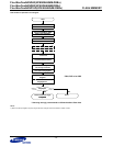
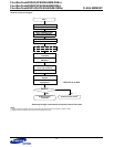
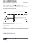
3.6.1 Superload Operation
See Timing Diagrams 6.10
The Superload operation is used to read multiple pages. During Superload operation, up to 4bit errors are corrected.
Once the first data is loaded, an interrupt status returns to ready. The data in DataRAM should be read after next Superload command is
issued. Data is being loaded from NAND to page buffer until whole data in DataRAM is read. The read from the DataRAM can be only syn-
chronous read mode. The status information related to load operation can be checked by the host if required. When host accesses DataRAM,
the address of DataRAM must be a multiple of 4.
Superload operation must be utilized within a same area partitioned as SLC or MLC.
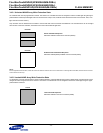
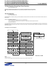
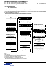
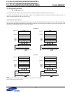
Superload Operation Flow Chart Diagram
NOTE :
1) FSA must be 00 and BSC must be 000 always for Superload operation.
2) BSA must be 1000.
3) In case of Superload operation, the number of sectors to be loaded is 8 sectors.
4) ‘Write 0 to interrupt register’ step may be ignored when using INT auto mode. Refer to chapter 2.8.18
5) For the first load, hosts must issue ‘Load(0000h)’ command.
6) In case of Superload operation, only synchronous read mode is valid.
Host should read data out until end of DataRAM(804FH).
After Reading out the last data(Add:804F), Additional clock should not be asserted.
Write ‘DFS, FBA’ of Flash
Add: F100h DQ=DFS*, FBA
Start
Write ‘FPA, FSA’ of Flash
Add: F107h DQ=FPA, FSA
1)
Write Load Command
Add=F220h DQ=0000h
5)
Wait for INT register or PIN
low to high transition
Add: F241h DQ[15]=INT
Host reads data from
DataRAM 0,1
6)
Wait for INT register or PIN
high to low transition
Add: F241h DQ[15]=INT
Superload Completed
NO
Finished to load
final page?
YES
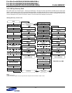
Select DataRAM for DDP
Add: F101h DQ=DBS*
* DBS, DFS is for DDP
Write 0 to INT register or PIN
4)
Add: F241h DQ=0000h
Write ‘DFS, FBA’ of Flash
Add: F100h DQ=FBA
Write ‘FPA, FSA’ of Flash
Add: F107h DQ=FPA, FSA
Write Superload Command
Add=F220h DQ=0003h
Write 0 to INT register or PIN
4)
Add: F241h DQ=0000h
Host reads data from
DataRAM 0,1
5)
Write ‘BSA
2)
, BSC’ of DataRAM
3)
Add: F200h DQ=0800h
Write System Configuration
Add: F221h DQ=ECC
Register
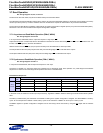
Read ECC Status Register1
Add: FF00h DQ=ER1[12:8], ER0[4:0]
Read ECC Status Register2
Add: FF01h DQ=ER3[12:8], ER2[4:0]
Read ECC Status Register3
Add: FF02h DQ=ER5[12:8], ER4[4:0]
Read ECC Status Register4
Add: FF03h DQ=ER7[12:8], ER6[4:0]
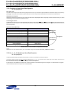
Read ECC Status Register1
Add: FF00h DQ=ER1[12:8], ER0[4:0]
Read ECC Status Register2
Add: FF01h DQ=ER3[12:8], ER2[4:0]
Read ECC Status Register3
Add: FF02h DQ=ER5[12:8], ER4[4:0]
Read ECC Status Register4
Add: FF03h DQ=ER7[12:8], ER6[4:0]