


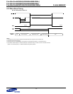

Flex-MuxOneNAND4G(KFM4GH6Q4M-DEBx)
- 140 -
FLASH MEMORY
Flex-MuxOneNAND8G(KFN8GH6Q4M-DEBx)
Flex-MuxOneNAND16G(KFKAGH6Q4M-DEBx)
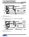
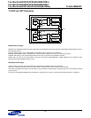
7.4 DDP and QDP Description
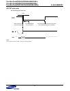
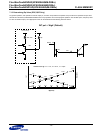
DDP(Dual Die Package):
8Gb DDP Flex-OneNAND contains two chips of 4Gb which are multiplexed such that they provide a single address range interface, with dou-
ble the storage capacity.
Since the address range is single, the BootRAM, the bufferRAM and the register set are multiplexed.
BootRAM: The bootRAM of chip1 is selected always, and the contents of the block 0 of chip1 are copied to it at startup.
DataRAM: DBS setting in Start Address2 Register(See Section 2.8.10) decides which DataRAM is selected.
Register Set: In the case of write, both registers in chip1 and chip2 will be written(Regardless of DBS). Reading out from register of chip1/
chip2 follows the DBS setting(See Section 2.8.10).
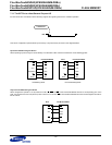
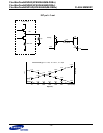
QDP(Quad Die Package):
A QDP is made up of 2 DDP chips and is effectively 2 separate Flex-OneNAND devices in the same die.
There are 2 chip select pins (CE1 and CE2) on a QDP device, using which one of the two devices can be selected.
Since there are separate chip-selects for the two devices, they have different address ranges and register sets which can be directly accessed
by the processor.
Thus each of the registers/BufferRAMs can be selected by using the CE pin, and then using the same settings that apply to a DDP chip.
Comp
Comp
DBS
DFS
DDP_OPT
GND
CE
CONTROL
LOGIC
SRAM
BUFFER
FLASH
CORE
Comp
Comp
DBS
DFS
DDP_OPT
V
DD
CE
CONTROL
LOGIC
SRAM
BUFFER
FLASH
CORE
CE INT
CHIP 1
CHIP 2
INT
INT