


Flex-MuxOneNAND4G(KFM4GH6Q4M-DEBx)
- 94 -
FLASH MEMORY
Flex-MuxOneNAND8G(KFN8GH6Q4M-DEBx)
Flex-MuxOneNAND16G(KFKAGH6Q4M-DEBx)
3.13.1 OTP Block Load Operation
An OTP Block Load Operation accesses the OTP area and transfers identified content from the OTP to the DataRAM on-chip buffer,
thus making the OTP contents available to the Host.
The OTP area is a separate part of the NAND Flash Array memory. It is accessed by issuing OTP Access command(65h) instead of
a Flash Block Address (FBA) value in Start Address1 Register.
.
After being accessed with the OTP Access Command, the contents of OTP memory area are loaded using the same operations as a normal
load operation to the NAND Flash Array memory (see section 3.6 for more information).
To exit the OTP access mode after an OTP Block Load Operation, a Cold-, Warm-, Hot-, or NAND Flash Core Reset operation is performed.
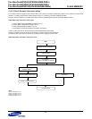
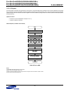
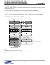
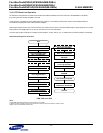
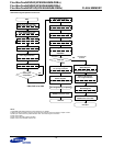
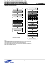
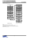
OTP Block Read Operation Flow Chart
NOTE :
1) FBA(NAND Flash Block Address) could be omitted or any address
2) ‘Write 0 to interrupt register’ step may be ignored when using INT auto mode. Refer to chapter 2.8.18.1
3) BSA must be 1000 and BSC must be 000.
Start
Wait for INT register
Add: F241h DQ[15]=INT
Write 0 to interrupt register
2)
Add: F241h DQ=0000h
Write ‘FPA, FSA’ of Flash
Add: F107h DQ=FPA, FSA
OTP Reading completed
Write ‘Load’ Command
Add: F220h
DQ=0000h
Wait for INT register
low to high transition
Add: F241h DQ[15]=INT
Write ‘OTP Access’ Command
Add: F220h DQ=0065h
Write ‘BSA, BSC’ of DataRAM
Add: F200h DQ=0800h
3)
low to high transition
OTP Exit
Host reads data from
DataRAM
Do Cold/Warm/Hot
/NAND Flash Core Reset
* DBS, DFS is for DDP
Write ‘DFS*, FBA’ of Flash
1)
Add: F100h DQ=DFS*, FBA
Write 0 to interrupt register
2)
Add: F241h DQ=0000h
Select DataRAM for DDP
Add: F101h DQ=DBS*