


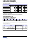

Flex-MuxOneNAND4G(KFM4GH6Q4M-DEBx)
- 59 -
FLASH MEMORY
Flex-MuxOneNAND8G(KFN8GH6Q4M-DEBx)
Flex-MuxOneNAND16G(KFKAGH6Q4M-DEBx)
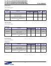
3.3.1 Cold Reset Mode Operation
See Timing Diagram 6.15
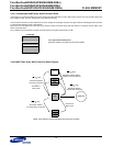
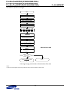
At system power-up, the voltage detector in the device detects the rising edge of Vcc and releases an internal power-up reset signal. This trig-
gers boot code loading. Bootcode loading means that the boot loader in the device copies designated sized data (1KB) from the beginning of
memory into the BootRAM. This sequence is the Cold Reset of Flex-MuxOneNAND.
The POR(Power On Reset) triggering level is typically 1.5V. Boot code copy operation activates 400us after POR.
Therefore, the system power should reach 1.7V within 400us from the POR triggering level for bootcode data to be valid.
It takes approximately 250us to copy 1KB of boot code. Upon completion of loading into the BootRAM, it is available to be read by the host.
The INT pin is not available until after IOBE = 1 and IOBE bit can be changed by host.
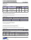
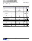
3.3.2 Warm Reset Mode Operation
See Timing Diagrams 6.16
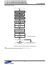
A Warm Reset means that the host resets the device by using the RP
pin. When the a RP low is issued, the device logic stops all current oper-
ations and executes internal reset operation and resets current NAND Flash core operation synchronized with the
falling edge of RP
.
During an Internal Reset Operation, the device initializes internal registers and makes output signals go to default status.
The BufferRAM data is kept unchanged after Warm/Hot reset operations.
The device guarantees the logic reset operation in case RP
pulse is longer than tRP min(200ns).
The device may reset if tRP < tRP min(200ns), but this is not guaranteed.
Warm reset will abort the current NAND Flash core operation. During a warm reset, the content of memory cells being altered is no longer
valid as the data will be partially programmed or erased.
Warm reset has no effect on contents of BootRAM and DataRAM.
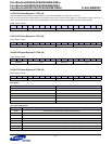
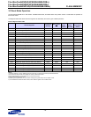
3.3.3 Hot Reset Mode Operation
See Timing Diagrams 6.17
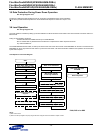
A Hot Reset means that the host resets the device by Reset command. The reset command can be either Command based or Register
Based. Upon receiving the Reset command, the device logic stops all current operation and executes an internal reset operation and resets
the current NAND Flash core operation.
During an Internal Reset Operation, the device initializes internal registers and makes output signals go to default status. The BufferRAM data
is kept unchanged after Warm/Hot reset operations.
Hot reset has no effect on contents of BootRAM and DataRAM.
3.3.4 NAND Flash Core Reset Mode Operation
See Timing Diagrams 6.18
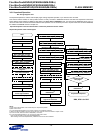
The Host can reset the NAND Flash Core operation by issuing a NAND Flash Core reset command. NAND Flash core reset will abort the cur-
rent NAND Flash core operation. During a NAND Flash core reset, the content of memory cells being altered is no longer valid as the data will
be partially programmed or erased.
NAND Flash Core Reset has an effect on neither contents of BootRAM and DataRAM nor register values.