


Flex-MuxOneNAND4G(KFM4GH6Q4M-DEBx)
- 89 -
FLASH MEMORY
Flex-MuxOneNAND8G(KFN8GH6Q4M-DEBx)
Flex-MuxOneNAND16G(KFKAGH6Q4M-DEBx)
3.12.1.3 PI Block Program Operation
The PI Block Program Operation accesses the PI area and programs content from the DataRAM on-chip buffer to the designated page(s) of
the PI.
A memory location in the PI area can be program.
The PI area is programmed using the same sequence as normal program operation after being accessed by the PI Block Access mode entry
command (see section 3.8 for more information).
Programming the PI Area
Issue the PI Access Command(Refer to Chapter 3.12.1.1).
Write data into the DataRAM
- In case of PI Lock(Add: 0200h, DQ=3XXXh
, The lower 10 bits[9:0] are boundary address) .
- In case of PI Unlock(Add: 0200h, DQ=FXXX
h, The lower 10 bits[9:0] are boundary address).
Write 0000h into Flash Block Address (FBA), that is address of NAND Flash Array address map.
Issue a Program command to program the data from the DataRAM into the PI.
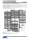
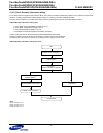
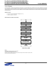
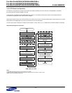
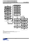
PI Block Program Operation Flow Chart (In PI Block Access Mode)
Locking the PI
Programming to PI block can be prevented by locking the PI area. Locking the PI area is accomplished by programming 3XXXh to 1st word of
sector0 of main of the page0 memory area in the PI block(XXXh out of 3XXXh is a boundary block address that ends SLC area).
Once Lock bits are programmed as lock status, PI block will be protected from program and erase. Boundary address is alterable before PI
block is locked, but it is not recommended.
At device power-up and PI Update operation, this word is updated internally. If 3XXXh is found(i.e. the status of PI is locked), Program/Erase
operations to PI block result in an error and the device updates the Error Bit of the Controller Status Register as "1"(fail).
NOTE :
1) Only the 1st word of 1st page of PI block (PI block Boundary Information) can be programmed in PI Block.
The rest of the block cannot be programmed.
2) FBA(NAND Flash Block Address) must be 0000h.
3) FPA must be 00h and FSA must be 00.
4) BSA must be 1000 and BSC must be 000.
5) ‘Write 0 to interrupt register’ step may be ignored when using INT auto mode. Refer to chapter 2.8.18.1
Start
Write ‘FPA, FSA’ of Flash
Add: F107h DQ=0000h
3)
Write Data into DataRAM
Add: 0200h DQ= 1 word
1)
PI Programming completed
Write Program command
DQ=0080h
Wait for INT register
low to high transition
Add: F241h DQ[15]=INT
Add: F220h
Write 0 to interrupt register
5)
Add: F241h DQ=0000h
NO
* DBS, DFS is for DDP
Read Controller
Status Register
Add: F240h
DQ[10]=1(Error)
YES
Write ‘BSA, BSC’ of DataRAM
Add: F200h DQ=0800h
4)
Write ‘DFS, FBA’ of Flash
Add: F100h DQ=FBA
2)
PI Program Error