


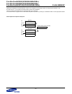
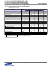

Flex-MuxOneNAND4G(KFM4GH6Q4M-DEBx)
- 111 -
FLASH MEMORY
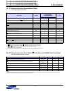
Flex-MuxOneNAND8G(KFN8GH6Q4M-DEBx)
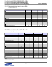
Flex-MuxOneNAND16G(KFKAGH6Q4M-DEBx)
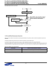
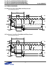
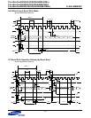
5.4 AC Characteristics for Synchronous Burst Read
See Timing Diagrams 6.1 and 6.2
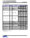
NOTE :
1) If OE
is disabled at the same time or before CE is disabled, the output will go to high-z by tOEZ.
If CE
is disabled at the same time or before OE is disabled, the output will go to high-z by tCEZ.
If CE
and OE are disabled at the same time, the output will go to high-z by tOEZ.
2) It is the following clock of address fetch clock.
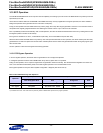
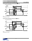
Parameter Symbol
66MHz 83MHz
Unit
Min Max Min Max
Clock CLK 1 66 1 83 MHz
Clock Cycle t
CLK 15 - 12 - ns
Initial Access Time t
IAA -70-70ns
Burst Access Time Valid Clock to Output Delay t
BA -11- 9ns
AVD
Setup Time to CLK tAVDS 5-4-ns
AVD
Hold Time from CLK tAVDH 2-2-ns
AVD
High to OE Low tAVDO 0-0-ns
Address Setup Time to CLK t
ACS 5-4-ns
Address Hold Time from CLK t
ACH 6-6-ns
Data Hold Time from Next Clock Cycle t
BDH 3-2-ns
Output Enable to Data t
OE -20-20ns
CE
Disable to Output & RDY High Z
t
CEZ
1)
-20-20ns
OE
Disable to Output High Z
t
OEZ
1)
-15-15ns
CE
Setup Time to CLK tCES 6 - 4.5 - ns
CLK High or Low Time t
CLKH/L tCLK/3 - 5 - ns
CLK
2)
to RDY valid
t
RDYO -11- 9ns
CLK to RDY Setup Time t
RDYA -11- 9ns
RDY Setup Time to CLK t
RDYS 4-3-ns
CE
low to RDY valid tCER -15-15ns