


Flex-MuxOneNAND4G(KFM4GH6Q4M-DEBx)
- 40 -
FLASH MEMORY
Flex-MuxOneNAND8G(KFN8GH6Q4M-DEBx)
Flex-MuxOneNAND16G(KFKAGH6Q4M-DEBx)
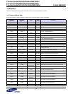
2.8.9 Start Address1 Register F100h (R/W)
This Read/Write register describes the NAND Flash block address which will be loaded, programmed, or erased.
F100h, default = 0000h
NOTE :
For QDP, See Section 7.4
Start Address1 Information
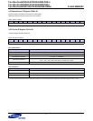
2.8.10 Start Address2 Register F101h (R/W)
This Read/Write register describes the method to select the BufferRAM of DDP (Device BufferRAM Select)
F101h, default = 0000h
Start Address2 Information
>DBS should be set to 1 when accessing the BufferRAM of the second chip(MSB chip) in a DDP.
>Since DDP chip has 2 BufferRAMs multiplexed, the BufferRAM which corresponds to the Flash core that is intended to be
accessed must be selected using DBS.
>Data in BufferRAM of one chip is not accessible to the Flash Core of the other chip in a DDP See Section 7.4.
2.8.11~15 Start Address3~7 Register F102h~F106h
This Register is reserved for future use.
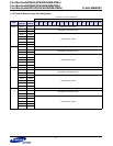
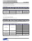
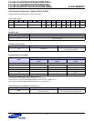
15 14 13 12 11 10 9 8 7 6 5 4 3 2 1 0
DFS Reserved(00000) FBA
Device Number of Block FBA
4Gb 1024 FBA[9:0]
8Gb DDP 2048 DFS[15] & FBA[9:0]
Register Information Description
FBA NAND Flash Block Address
DFS Flash Core of DDP (Device Flash Core Select)
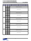
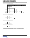
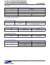
15 14 13 12 11 10 9 8 7 6 5 4 3 2 1 0
DBS Reserved(000000000000000)
Register Information Description
DBS BufferRAM and Register of DDP (Device BufferRAM Select)