


Flex-MuxOneNAND4G(KFM4GH6Q4M-DEBx)
- 70 -
FLASH MEMORY
Flex-MuxOneNAND8G(KFN8GH6Q4M-DEBx)
Flex-MuxOneNAND16G(KFKAGH6Q4M-DEBx)
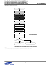
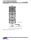
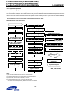
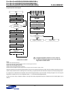
3.7.2.3 Programmable Burst Read Latency Operation
See Timing Diagrams 6.1 and 6.2
Upon power up, the number of initial clock cycles from Valid Address (AVD
) to initial data defaults to four clocks.
The number of clock cycles (n) which are inserted after the clock which is latching the address. The host can read the first data with the
(n+1)th rising edge.
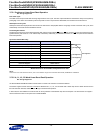
The number of total initial access cycles is programmable from three to seven cycles. After the number of programmed burst clock cycles is
reached, the rising edge of the next clock cycle triggers the next burst data.
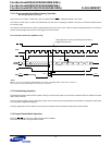
Four Clock Burst Read Latency (BRWL=4 case)
*
NOTE :
BRWL=4, HF=0 is recommended for 40MHz~66MHz. For frequency over 66MHz, BRWL should be 6 or 7 while HF=1.
Also, for frequency under 40MHz, BRWL can be reduced to 3, and HF=0.
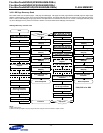
3.7.3 Handshaking Operation
The handshaking feature allows the host system to simply monitor the RDY signal from the device to determine when the initial word of burst
data is ready to be read.
To set the number of initial cycles for optimal burst mode, the host should use the programmable burst read latency configuration (see section
2.8.19, "System Configuration1 Register").
The rising edge of RDY which is derived at one cycle prior of data fetch clock indicates the initial word of valid burst data.
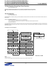
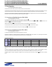
3.7.4 Output Disable Mode Operation
When the CE or OE input is at V
IH
, output from the device is disabled.
The outputs are placed in the high impedance state.
tIAA
Hi-Z
CE
CLK
AVD
OE
RDY
tRDYA
A/DQ0:
A/DQ15
D6 D7 D0 D1 D2 D3 D7 D0
Hi-Z
Valid
Address
-10123
tBA
Rising edge of the clock cycle following last read latency
triggers next burst data
tRDYS
4