


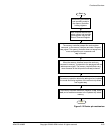

Functional Overview
ARM DDI 0389B Copyright © 2006 ARM Limited. All rights reserved. 2-21
memory bursts, terminating a memory transfer at the burst boundary. Also ensure the
page size is an integer multiple of the burst length, to avoid a memory burst crossing a
page boundary.
When the burst_align bit is not set, the SMC ignores the memory burst boundary when
mapping commands onto memory commands. This setting is intended for use with
devices such as NOR flash. These devices have no concept of pages.
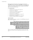
Memory burst length
The SMC enables you to program the memory burst length on an individual chip basis,
from length 1 to 32 beats, or a continuous burst. However, the length of memory bursts
are limited by the size of the read and write data FIFOs, and the programmed memory
burst must not exceed this upper limit.
For read transfers, the maximum memory burst length is the depth of the read data
FIFO, and it is four. For writes, the burst length is the depth of the write FIFO, and is
four.
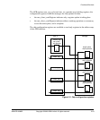
Booting using the SRAM
The SMC enables the lowest SRAM chip select, normally chip 0, to be bootable. To
enable SRAM memory to be bootable, the SRAM interface does not require any special
functionality, other than knowing the memory width of the memory concerned. This is
indicated by a top-level tie-off. To enable the SMC to work with the slowest memories
the timing registers reset to the worst case values. When the smc_remap_0 port signal
is HIGH, the memory with the bootable chip select is set by the smc_sram_mw_0[1:0]
tie-off port signal.
Additionally, while the SMC input smc_remap_0 is HIGH, the bootable chip is aliased
to base address
0x0
.