


Programmer’s Model
ARM DDI 0389B Copyright © 2006 ARM Limited. All rights reserved. 3-17
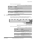
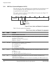
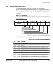
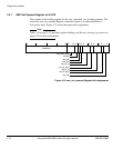
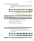
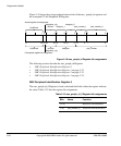
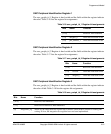
Table 3-11 lists the register bit assignments.
Table 3-11 smc_opmode Register bit assignments
Bits Name Function
[31:24] address_match Returns the value of this tie-off. This is the comparison value for address bits [31:24] to
determine the chip that is selected.
[23:16] address_mask Returns the value of this tie-off. This is the mask for address bits[31:24] to determine the
chip that must be selected. A logic 1 indicates the bit is used for comparison.
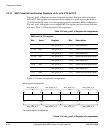
[15:13] burst_align These bits determine whether memory bursts are split on memory burst boundaries:
000 = bursts can cross any address boundary
001 = burst split on memory burst boundary, that is, 32 beats for continuous
010 = burst split on 64 beat boundary
011 = burst split on 128 beat boundary
100 = burst split on 256 beat boundary
others = reserved.
Note
For asynchronous transfers:
• the AHB MC always aligns read bursts to the memory burst boundary, when
rd_sync = 0
• the AHB MC always aligns write bursts to the memory burst boundary, when
wr_sync = 0.
[12] bls This bit affects the assertion of the byte-lane strobe outputs:
b0 = bls timing equals chip select timing. This is the default setting.
b1 = bls timing equals smc_we_n_0 timing. This setting is used for 8-bit memories that have
no Byte Lane Strobe inputs. In this case, the smc_bls_n_0[3:0] output of the memory
controller is connected to the smc_we_n_0 memory input.
[11] adv The memory uses the address advance signal smc_adv_n_0 when set.
[10] baa The memory uses the burst advance signal smc_baa_n_0 when set.
[9:7] wr_bl Determines the memory burst length for writes:
b000 = 1 beat
b001 = 4 beats
b010 = 8 beats
b011 = 16 beats
b100 = 32 beats
b101 = continuous
b110-b111 = reserved.