


Programmer’s Model
3-16 Copyright © 2006 ARM Limited. All rights reserved. ARM DDI 0389B
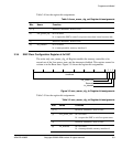
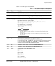
Table 3-10 lists the register bit assignments.
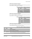
3.3.10 SMC Opmode Registers <0-3> at 0x1104, 0x1124, 0x1144, 0x1164
There is an instance of the smc_opmode Register for each chip supported. This register
is read-only and cannot be read in the Reset state.
The reset values of these registers are configuration-dependent. You can set the memory
width for the chip select 0 of each memory interface with a tie off to enable booting from
that chip. The reset value of memory width for all other chip selects is the configured
width. You must set all other bits to
0x0
, apart from address_match and address_mask.
These are set by tie-offs at the top level.
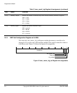
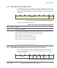
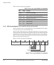
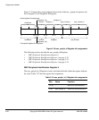
Figure 3-15 shows the register bit assignments.
Figure 3-15 smc_opmode Register bit assignments
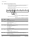
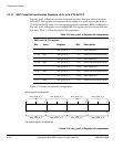
Table 3-10 smc_sram_cycles Register bit assignments
Bits Name Function
[31:20] - Reserved, read undefined
[19:17] t_tr Turnaround time for SRAM chip configuration
[16:14] t_pc Page cycle time for SRAM chip configuration
[13:11] t_wp smc_we_n assertion delay
[10:8] t_ceoe smc_oe_n assertion delay for SRAM chip configurations
[7:4] t_wc Write cycle time
[3:0] t_rc Read cycle time
PZUGBEODGGUHVVBPDVNDGGUHVVBPDWFK
UGBV\QF
ZUBV\QF
ZUBEO
EDD
EOV
DGY
EXUVWBDOLJQ