Programmer’s Model
ARM DDI 0389B Copyright © 2006 ARM Limited. All rights reserved. 3-5
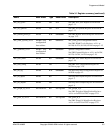
smc_set_cycles
0x1014
WO N/A See SMC Set Cycles Register at 0x1014 on
page 3-11.
smc_set_opmode
0x1018
WO N/A See SMC Set Opmode Register at 0x1018 on
page 3-12.
smc_refresh_period_0
0x1020
R/W
0x00000000
See SMC Refresh Period 0 Register at 0x1020
on page 3-15.
smc_sram_cycles0_<0-3>
0x1000
+ chip
configuration
base address
RO
0x0002B3CC
smc_sram_cycles configuration where:
See SMC SRAM Cycles Registers <0-3> at
0x1100, 0x1120, 0x1140, 0x1160 on page 3-15.
smc_opmode0_<0-3>
0x1004 +
chip
configuration
base address
RO
0x00000802
opmode configuration where:
See SMC Opmode Registers <0-3> at 0x1104,
0x1124, 0x1144, 0x1164 on page 3-16.
smc_user_status
0x1200
RO
0x00000000
See SMC User Status Register at 0x1200 on
page 3-18.
smc_user_config
0x1204
WO - See SMC User Configuration Register at
0x1204 on page 3-19.
smc_int_cfg
0x1E00
R/W
0x00000000
See SMC Integration Configuration Register at
0x1E00 on page 4-2.
smc_int_inputs
0x1E04
RO - See Integration Inputs Register at 0x1E04 on
page 4-3.
smc_int_outputs
0x1E08
WO - See Integration Outputs Register at 0x1E08 on
page 4-4.
smc_periph_id_<0-3>
0x1FE0-0x1FEC
RO See registers smc_periph_id_n
See SMC Peripheral Identification Registers
<0-3> at 0x1FE0-0x1FEC on page 3-19.
smc_pcell_id_<0-3>
0x1FF0-0x1FFC
RO See registers smc_pcell_id_n
See SMC PrimeCell Identification Registers
<0-3> at 0x1FF0-0x1FFC on page 3-22.
Table 3-1 Register summary (continued)
Name Base offset Type Reset value Description


