


Functional Overview
2-36 Copyright © 2006 ARM Limited. All rights reserved. ARM DDI 0389B
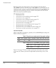
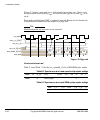
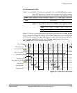
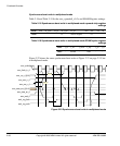
Synchronous burst write in multiplexed-mode
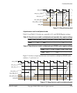
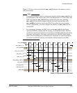
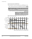
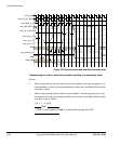
Table 2-18 and Table 2-19 list the smc_opmode0_<0-3> and SRAM Register settings.
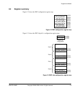
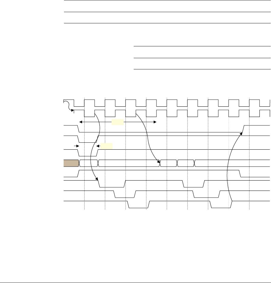
Figure 2-22 shows the same synchronous burst write as Figure 2-21 on page 2-35, but
in multiplexed-mode.
Figure 2-22 Synchronous burst write in multiplexed-mode
Table 2-18 Synchronous burst write in multiplexed-mode opmode chip register
settings
Field mw rd_sync rd_bl wr_sync wr_bl baa adv bls ba
Value - - - b1 <burst length> - b1 - -
Table 2-19 Synchronous burst write in multiplexed-mode SRAM cycles register
settings
Field t_rc t_wc t_ceoe t_wp t_pc t_tr
Value - b0100 - b001 - -
VPFBFVBQB>@
VPFBDGYBQB
VPFBZHBQB
VPFBGDWDBRXWB>@
VPFBGDWDBHQB
VPFBZDLWB
ZDLWBUHJBPFON
$
ZDLWBUHJBIEFON
VPFBPFON
VPFBIEFONBLQB
W
:&
W
:3
' ' '