


Programmer’s Model
3-4 Copyright © 2006 ARM Limited. All rights reserved. ARM DDI 0389B
Note
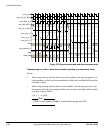
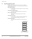
Figure 3-3 on page 3-3 shows the maximum number of supported chips. If you intend
to use fewer, then the highest chip configuration blocks of the correct type are read back
as zero.
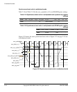
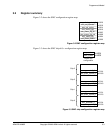
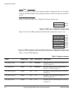
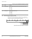
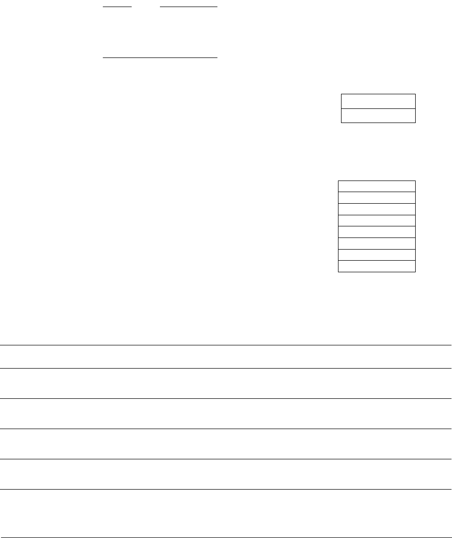
Figure 3-4 shows the SMC user configuration memory register map.
Figure 3-4 SMC user configuration register map
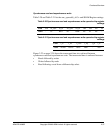
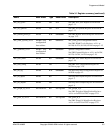
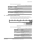
Figure 3-5 shows the SMC peripheral and PrimeCell configuration register map.
Figure 3-5 SMC peripheral and PrimeCell identification configuration register map
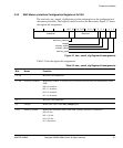
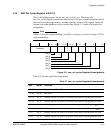
Table 3-1 lists the SMC Registers.
VPFBXVHUBFRQILJ
VPFBXVHUBVWDWXV
[
[
VPFBSFHOOBLGB
VPFBSFHOOBLGB
VPFBSFHOOBLGB
VPFBSFHOOBLGB
VPFBSHULSKBLGB
VPFBSHULSKBLGB
VPFBSHULSKBLGB
VPFBSHULSKBLGB
[))&
[))
[))
[))
[)(&
[)(
[)(
[)(
Table 3-1 Register summary
Name Base offset Type Reset value Description
smc_memc_status
0x1000
RO
0x00000000
See SMC Memory Controller Status Register at
0x1000 on page 3-6.
smc_memif_cfg
0x1004
RO
0x0000002D
See SMC Memory Interface Configuration
Register at 0x1004 on page 3-7.
smc_memc_cfg_set
0x1008
WO N/A See SMC Set Configuration Register at 0x1008
on page 3-8.
smc_memc_cfg_clr
0x100C
WO N/A See SMC Clear Configuration Register at
0x100C on page 3-9.
smc_direct_cmd
0x1010
WO N/A See SMC Direct Command Register at 0x1010
on page 3-10.