


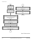

Functional Overview
2-30 Copyright © 2006 ARM Limited. All rights reserved. ARM DDI 0389B
Note
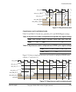
In multiplexed-mode, both address and data are output by the SMC on the
smc_data_out_0[31:0] output bus. Read data is accepted on the smc_data_in_0[31:0]
bus.
Asynchronous write
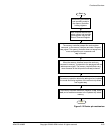
Table 2-6 and Table 2-7 list the smc_opmode0_<0-3> and SRAM Register settings.
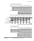
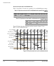
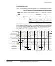
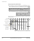
Figure 2-16 shows an asynchronous write with a write cycle time t
WC
of four cycles and
a smc_we_n_0 assertion duration, t
WP
, of two cycles.
Note
The timing parameter t
WC
is controlling the deassertion of smc_we_n_0. You can use
it to vary the hold time of smc_cs_n_0[3:0], smc_add_0[31:0] and
smc_data_out_0[31:0]. This differs from the read case where the timing parameter
t
CEOE
controls the delay in the assertion of smc_oe_n_0. Additionally, smc_we_n_0 is
always asserted one cycle after smc_cs_n_0[3:0] to ensure the address bus is valid.
Figure 2-16 Asynchronous write
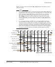
Table 2-6 Asynchronous write opmode chip register settings
Field mw rd_sync rd_bl wr_sync wr_bl baa adv bls ba
Value - - - b0 b000 - - - -
Table 2-7 Asynchronous write SRAM cycles register settings
Field t_rc t_wc t_ceoe t_wp t_pc t_tr
Value - b0100 - b010 - -
VPFBFVBQB>@
VPFBZHBQB
VPFBDGGB>@
VPFBGDWDBRXWB>@
VPFBPFON
W
:&
W
:3
$
'