


Programmer’s Model
3-14 Copyright © 2006 ARM Limited. All rights reserved. ARM DDI 0389B
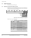
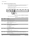
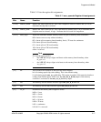
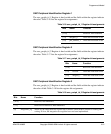
[9:7] set_wr_bl Holding register for value to be written to the specific SRAM chip smc_opmode Register bls
field.
Encodes the memory burst length:
b000 = 1 beat
b001 = 4 beats
b010 = 8 beats
b011 = 16 beats
b100 = 32 beats
b101 = continuous
b110-b111 = reserved.
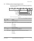
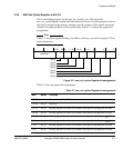
[6] set_wr_sync Holding register for value to be written to the specific SRAM chip smc_opmode Register
wr_sync field. The memory writes are synchronous when set. This bit is reserved for a
NAND memory interface.
[5:3] set_rd_bl Holding register for value to be written to the specific SRAM chip smc_opmode Register bls
field.
Encodes the memory burst length:
b000 = 1 beat
b001 = 4 beats
b010 = 8 beats
b011 = 16 beats
b100 = 32 beats
b101 - continuous
b110-b111 = reserved.
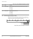
[2] set_rd_sync Holding register before being written to the specific SRAM chip smc_opmode Register
rd_sync field. Memory in sync mode when set.
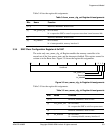
[1:0] set_mw Holding register for value to be written to the specific SRAM chip smc_opmode Register
memory width (mw) field.
Encodes the memory data bus width:
b00 = 8 bits
b01 = 16 bits
b10 = 32 bits
b11 = reserved.
You can program this to the configured width or half that width. See SMC Memory Interface
Configuration Register at 0x1004 on page 3-7.
Table 3-8 smc_set_opmode Register bit assignments (continued)
Bits Name Function