Functional Overview
ARM DDI 0389B Copyright © 2006 ARM Limited. All rights reserved. 2-35
Synchronous burst write
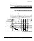
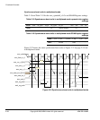
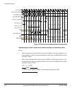
Table 2-16 and Table 2-17 list the smc_opmode0_<0-3> and SRAM Register settings.
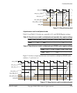
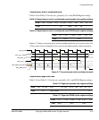
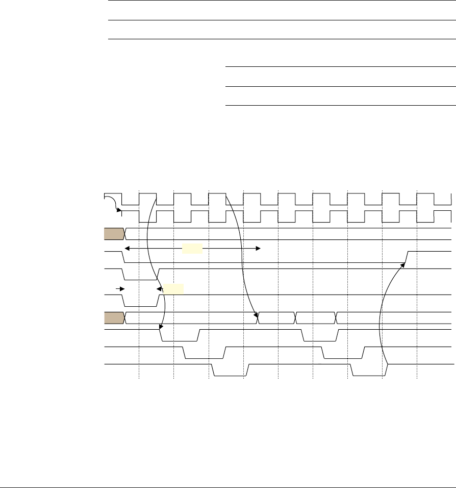
Figure 2-21 shows a synchronous burst write transfer that is delayed by the smc_wait_0
signal. You must configure the memory to assert smc_wait_0 one cycle early and with
an active LOW priority. The smc_wait_0 signal is again registered with the fed back
clock and smc_mclk0 before being used. The smc_wait_0 signal is used in the
smc_mclk0 domain to the memory interface FSM.
Figure 2-21 Synchronous burst write
Table 2-16 Synchronous burst write opmode chip register settings
Field mw rd_sync rd_bl wr_sync wr_bl baa adv bls ba
Value - - - b1 <burst length> - b1 - -
Table 2-17 Synchronous burst write SRAM cycles register settings
Field t_rc t_wc t_ceoe t_wp t_pc t_tr
Value - b0100 - b001 - -
VPFBDGGB>@
VPFBFVBQB>@
VPFBDGYBQB
VPFBZHBQB
VPFBGDWDBRXWB>@
VPFBZDLWB
ZDLWBUHJBIEFON
ZDLWBUHJBPFON
VPFBPFON
VPFBIEFONBLQB
W
:&
$''5
' ' ' '
W
:3


