


Programmer’s Model
ARM DDI 0389B Copyright © 2006 ARM Limited. All rights reserved. 3-15
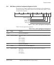
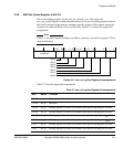
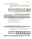
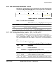
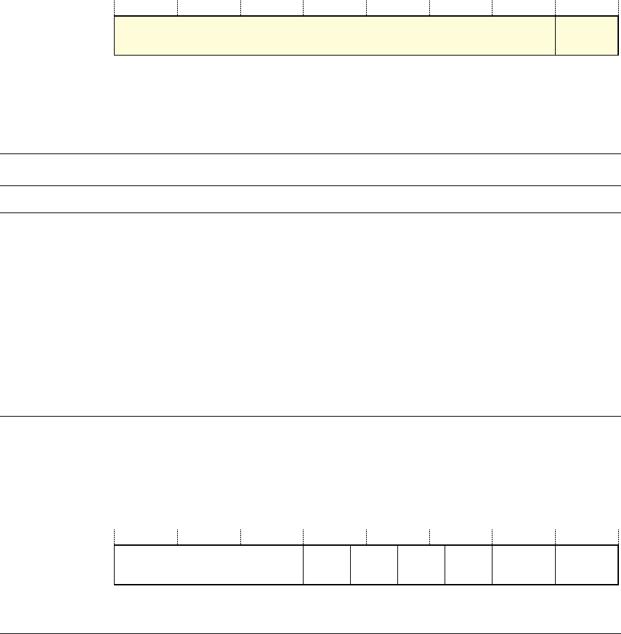
3.3.8 SMC Refresh Period 0 Register at 0x1020
The read/write smc_refresh_period_0 Register enables the AHB MC to perform refresh
cycles for PSRAM devices that you connect to memory interface 0. You cannot access
this register in either the Reset or low-power states. Figure 3-13 shows the register bit
assignments.
Figure 3-13 smc_refresh_period_0 Register bit assignments
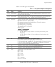
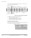
Table 3-9 lists the register bit assignments.
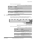
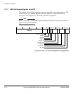
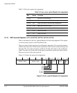
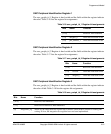
3.3.9 SMC SRAM Cycles Registers <0-3> at 0x1100, 0x1120, 0x1140, 0x1160
There is an instance of this register for each SRAM chip supported. The read-only
smc_sram_cycles Register cannot be read in the Reset state. Figure 3-14 shows the
register bit assignments.
Figure 3-14 smc_sram_cycles Register bit assignments
8QGHILQHG
SHULRG
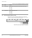
Table 3-9 smc_refresh_period_0 Register bit assignments
Bits Name Function
[31:4] - Reserved, read undefined.
[3:0] period Sets the number of consecutive memory bursts that are permitted, prior to the AHB MC deasserting
chip select to enable the PSRAM to initiate a refresh cycle. The options are:
b0000 = disables the insertion of idle cycles between consecutive bursts
b0001 = an idle cycle occurs after each burst
b0010 = an idle cycle occurs after 2 consecutive bursts
b0011 = an idle cycle occurs after 3 consecutive bursts
b0100 = an idle cycle occurs after 4 consecutive bursts
.
.
.
b1111 = an idle cycle occurs after 15 consecutive bursts.
WBUFWBZFWBFHRHWBZSWBSFWBWU8QGHILQHG