


Functional Overview
2-32 Copyright © 2006 ARM Limited. All rights reserved. ARM DDI 0389B
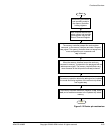
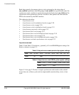
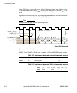
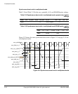
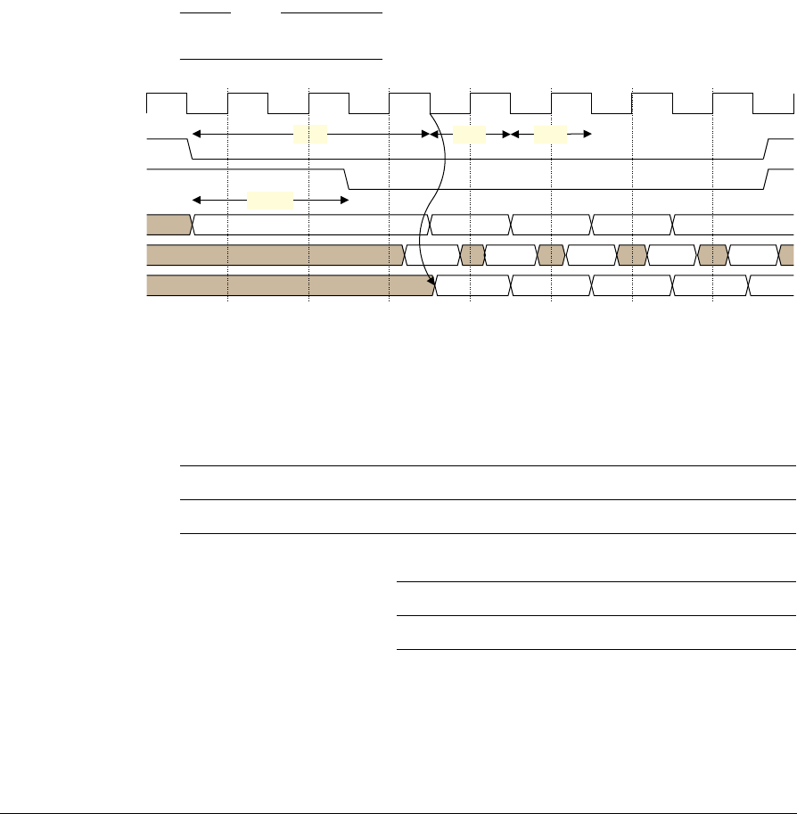
Figure 2-18 shows a page read access, with an initial access time, t
RC
, of three cycles,
an output enable assertion delay, t
CEOE
, of two cycles and a page access time, t
PC
, of one
cycle.
Page mode is enabled in the SMC by setting the opmode Register for the relevant chip
to asynchronous reads and the burst length to the page size.
Note
Multiplexed-mode page accesses are not supported.
Figure 2-18 Page read
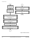
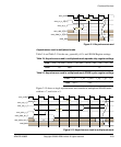
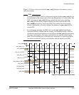
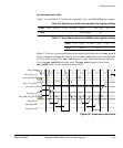
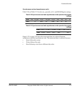
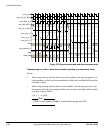
Synchronous burst read
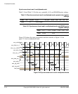
Table 2-12 and Table 2-13 list the smc_opmode0_<0-3> and SRAM Register settings.
VPFBFVBQB>@
VPFBRHBQB
VPFBDGGB>@
VPFBGDWDBLQB>@
UHDGBGDWD
VPFBPFON
$
'
$ $ $
' ' ' '
' ' ' ' '
W
5&
W
3&
W
3&
W
&(2(
$
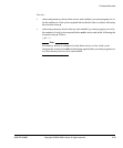
Table 2-12 Synchronous burst read opmode chip register settings
Field mw rd_sync rd_bl wr_sync wr_bl baa adv bls ba
Value - b1 <burst length> - - - b1 - -
Table 2-13 Synchronous burst read SRAM cycles register settings
Field t_rc t_wc t_ceoe t_wp t_pc t_tr
Value b0100 - b010 - - -