


List of Figures
viii Copyright © 2006 ARM Limited. All rights reserved. ARM DDI 0389B
Figure 2-20 Synchronous burst read in multiplexed-mode ........................................................ 2-34
Figure 2-21 Synchronous burst write ......................................................................................... 2-35
Figure 2-22 Synchronous burst write in multiplexed-mode ........................................................ 2-36
Figure 2-23 Synchronous read and asynchronous write ............................................................ 2-38
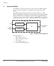
Figure 3-1 SMC register map ..................................................................................................... 3-2
Figure 3-2 SMC configuration register map ............................................................................... 3-3
Figure 3-3 SMC chip configuration register map ........................................................................ 3-3
Figure 3-4 SMC user configuration register map ....................................................................... 3-4
Figure 3-5 SMC peripheral and PrimeCell identification configuration register map .................. 3-4
Figure 3-6 smc_memc_status Register bit assignments ........................................................... 3-6
Figure 3-7 smc_memif_cfg Register bit assignments ................................................................ 3-7
Figure 3-8 smc_memc_cfg_set Register bit assignments ......................................................... 3-8
Figure 3-9 smc_memc_cfg_clr Register bit assignments .......................................................... 3-9
Figure 3-10 smc_direct_cmd Register bit assignments ............................................................. 3-10
Figure 3-11 smc_set_cycles Register bit assignments .............................................................. 3-11
Figure 3-12 smc_set_opmode Register bit assignments ........................................................... 3-12
Figure 3-13 smc_refresh_period_0 Register bit assignments .................................................... 3-15
Figure 3-14 smc_sram_cycles Register bit assignments ........................................................... 3-15
Figure 3-15 smc_opmode Register bit assignments .................................................................. 3-16
Figure 3-16 smc_user_status Register bit assignments ............................................................ 3-18
Figure 3-17 smc_user_config Register bit assignments ............................................................ 3-19
Figure 3-18 smc_periph_id Register bit assignments ................................................................ 3-20
Figure 3-19 smc_pcell_id Register bit assignments ................................................................... 3-22
Figure 4-1 SMC integration test register map ............................................................................ 4-2
Figure 4-2 smc_int_cfg Register bit assignments ...................................................................... 4-2
Figure 4-3 smc_int_inputs Register bit assignments ................................................................. 4-3
Figure 4-4 smc_int_outputs Register bit assignments ............................................................... 4-4
Figure 5-1 SMC and memory initialization sheet 1 of 3 ............................................................. 5-3
Figure 5-2 SMC and memory initialization sheet 2 of 3 ............................................................. 5-4
Figure 5-3 SMC and memory initialization sheet 3 of 3 ............................................................. 5-5
Figure A-1 AHB MC PL241 grouping of signals ......................................................................... A-2