


Functional Overview
ARM DDI 0389B Copyright © 2006 ARM Limited. All rights reserved. 2-33
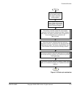
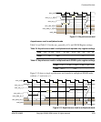
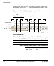
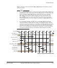
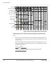
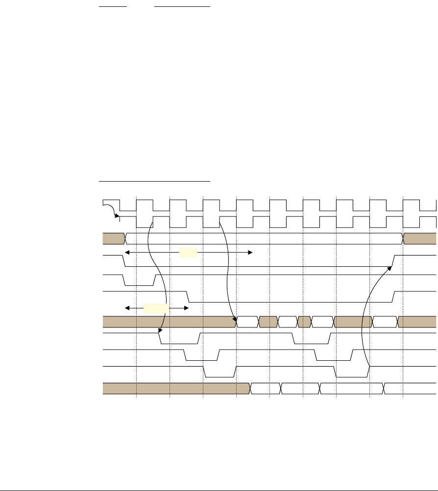
Figure 2-19 shows a burst read with the smc_wait_0 output of the memory used to
delay the transfer.
Note
• Synchronous memories have a configuration register enabling smc_wait_0 to be
asserted either on the same clock cycle as the delayed data or a cycle earlier. The
SMC only supports smc_wait_0 being asserted one cycle early, enabling
smc_wait_0 to be initially sampled with the fed back clock and then with
smc_mclk0 before being used by the FSM. This enables the easiest timing
closure. Additionally, you must configure the memory for smc_wait_0 to be
active LOW.
• In synchronous operation, the SMC relies on the smc_wait_0 signal being
deasserted HIGH to indicate that the memory can finish the transfer. When in
synchronous mode some memories do not deassert the smc_wait_0 signal during
non-array read transfers. Non-array read transfers are typically status register
reads. To avoid stalling the system with these memories, in synchronous mode
you must not perform non-array read transfers with the memory and SMC.
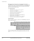
Figure 2-19 Synchronous burst read
VPFBDGGUHVV $''5
VPFBFVBQB>@
VPFBDGYBQB
VPFBRHBQB
VPFBGDWDBLQB>@ ' ' ' '
VPFBZDLWB
ZDLWBUHJBIEFON
UHDGBGDWD
' ' '
ZDLWBUHJBPFON
VPFBPFON
VPFBIEFONBLQB
'
W
5&
W
&(2(