Glueless four-processor connection with minimum latency
Snooping cache coherency
Four-way superscalar design with nine execution units; four integer execution
units
Three floating-point execution units
Two graphics execution units
Selectable little- or big-endian byte ordering
64-bit address pointers
16-Kbyte non-blocking data cache
16-Kbyte instruction cache; single cycle branch following
Power management
Software prefetch instruction support
Multiple outstanding requests
C.1.4 Memory System
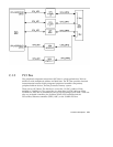
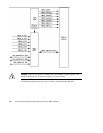
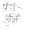
The memory system consists of three components: the QSC ASIC, the XB9+ ASIC,
and the memory module. The QSC ASIC generates memory addresses and control
signals to the memory module. The QSC ASIC also coordinates the data transfers
among the DIMMs through two 144-bit-wide processor data buses
(UPA_DATABUS0) and the 72-bit-wide I/O data bus (UPA_DATABUS1).
DIMMs are organized in banks in groups of four (quads). DIMM capacities of
32-Mbyte, 64-Mbyte, and 128-Mbyte are supported by the memory module. When all
DIMM banks are populated with 128-Mbyte DIMMs, maximum memory capacity is
2 Gbytes.
Organizing the four DIMM banks with 128-Mbyte (plus ECC bit) DIMMs allows data
streams to be transferred on a 512-bit-wide (plus ECC) memory data bus. The XB9+
ASIC coordinates all buses, which include the following: memory data, UPA_DATA0,
UPA_DATA1, UPA_DATA2, and UPA_DATA3.
The memory module is arranged in four banks. DIMMs are always accessed four at a
time. Consequently, the DIMMs must be installed in groups of four (quad) and
individual DIMMs within a bank must be of equal capacity.
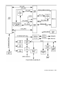
The following figure illustrates the memory module functional block diagram.
Functional Description 255


